Zxmp3f30fh new prod uc t, Electrical characteristics, Zxmp3f30fh – Diodes ZXMP3F30FH User Manual
Page 3
ZXMP3F30FH
Document number: DS33579 Rev. 2 - 2
3 of 7
February 2014
© Diodes Incorporated
ZXMP3F30FH
NEW PROD
UC
T
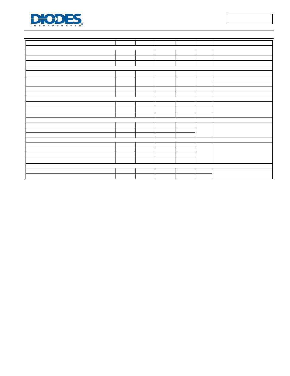
Electrical Characteristics
(@T
A
= +25°C, unless otherwise specified.)
Characteristic Symbol
Min
Typ
Max
Unit
Test
Condition
OFF CHARACTERISTICS
Drain-Source Breakdown Voltage
BV
DSS
-30
⎯
⎯
V
V
GS
= 0V, I
D
= -250μA
Zero Gate Voltage Drain Current
I
DSS
⎯
⎯
-1 nA
V
DS
= -30V, V
GS
= 0V
Gate-Source Leakage
I
GSS
⎯
⎯
±100
nA
V
GS
=
±20V, V
DS
= 0V
ON CHARACTERISTICS
Gate Threshold Voltage
V
GS(th)
-1
⎯
-3 V
V
DS
= V
GS
, I
D
= -250μA
Static Drain-Source On-Resistance (Note 9)
R
DS (ON)
⎯
⎯
80
140
mΩ
V
GS
= -10V, I
D
= -2.5A
V
GS
= -4.5V, I
D
= -1.9A
Forward Transconductance (Note 9 & 10)
g
fs
⎯
5
⎯
S
V
DS
= -15V, I
D
= -3A
Diode Forward Voltage (Note 9)
V
SD
⎯
-0.8 -1.2 V
V
GS
= 0V, I
S
= -1.7A
DYNAMIC CHARACTERISTICS (Note 10)
Input Capacitance
C
iss
⎯
370
⎯
pF
V
DS
= -15V, V
GS
= 0V,
f = 1.0MHz
Output Capacitance
C
oss
⎯
72
⎯
pF
Reverse Transfer Capacitance
C
rss
⎯
38
⎯
pF
GATE CHARACTERISTICS
Total Gate Charge
Qg
⎯
7
⎯
nC
V
DS
= -15V, V
GS
= -10V,
I
D
= -3A
Gate-Source Charge
Q
gs
⎯
1.2
⎯
Gate-Drain Charge
Q
gd
⎯
1.3
⎯
SWITCHING CHARACTERISTICS (Note 10 & 11)
Turn-On Delay Time
t
d(on)
⎯
1.3
⎯
ns
V
DS
= -15V, V
GS
= -10V,
I
D
= -1A, R
G
= 6.0Ω
Rise Time
t
r
⎯
2.6
⎯
Turn-On Delay Time
t
d(off)
⎯
49
⎯
Rise Time
t
f
⎯
22
⎯
SOURCE-DRAIN DIODE CHARACTERISTICS (Note 11)
Reverse Recovery Time
t
rr
⎯
14.6
⎯
ns
IS= -1.5A,di/dt=100A/μs
Reverse Recovery Charge
Q
rr
⎯
9.5
⎯
nC
Notes:
5. For a device surface mounted on 25mm x 25mm x 1.6mm FR4 PCB with high coverage of single sided 1oz copper, in still air conditions.
6. Mounted on FR4 PCB measured at t
≤10 sec.
7. Repetitive rating on 25mm x 25mm FR4 PCB, D=0.02, pulse width 300
μs – pulse width limited by maximum junction temperature.
8. Thermal resistance from junction to solder-point (at the end of the drain lead).
9. Measured under pulsed conditions. Pulse width ≤ 300μs; duty cycle ≤ 2%.
10. Switching characteristics are independent of operating junction temperature.
11. For design aid only, not subject to production testing.