Diodes ZVP2106A User Manual
Zvp2106a, P-channel enhancement mode vertical dmos fet, Typical characteristics
P-CHANNEL ENHANCEMENT
MODE VERTICAL DMOS FET
ISSUE 2 – MARCH 94
FEATURES
*
60 Volt V
DS
*
R
DS(on)
=5
Ω
ABSOLUTE MAXIMUM RATINGS.
PARAMETER
SYMBOL
VALUE
UNIT
Drain-Source Voltage
V
DS
-60
V
Continuous Drain Current at T
amb
=25°C
I
D
-280
mA
Pulsed Drain Current
I
DM
-4
A
Gate Source Voltage
V
GS
±
20
V
Power Dissipation at T
amb
=25°C
P
tot
700
mW
Operating and Storage Temperature Range
T
j
:T
stg
-55 to +150
°C
ELECTRICAL CHARACTERISTICS (at T
amb
= 25°C unless otherwise stated).
PARAMETER
SYMBOL MIN.
MAX. UNIT
CONDITIONS.
Drain-Source Breakdown
Voltage
BV
DSS
-60
V
I
D
=-1mA, V
GS
=0V
Gate-Source Threshold
Voltage
V
GS(th)
-1.5
-3.5
V
ID=-1mA, V
DS
= V
GS
Gate-Body Leakage
I
GSS
20
nA
V
GS
=
±
20V, V
DS
=0V
Zero Gate Voltage Drain
Current
I
DSS
-0.5
-100
µ
A
µ
A
V
DS
=-60 V, V
GS
=0
V
DS
=-48 V, V
GS
=0V, T=125°C
(2)
On-State Drain Current(1)
I
D(on)
-1
A
V
DS
=-18 V, V
GS
=-10V
Static Drain-Source On-State
Resistance (1)
R
DS(on)
5
Ω
V
GS
=-10V,I
D
=-500mA
Forward Transconductance
(1)(2)
g
fs
150
mS
V
DS
=-18V,I
D
=-500mA
Input Capacitance (2)
C
iss
100
pF
Common Source Output
Capacitance (2)
C
oss
60
pF
V
DS
=-18V, V
GS
=0V, f=1MHz
Reverse Transfer
Capacitance (2)
C
rss
20
pF
Turn-On Delay Time (2)(3)
t
d(on)
7
ns
V
DD
≈
-18V, I
D
=-500mA
Rise Time (2)(3)
t
r
15
ns
Turn-Off Delay Time (2)(3)
t
d(off)
12
ns
Fall Time (2)(3)
t
f
15
ns
(1) Measured under pulsed conditions. Width=300
µ
s. Duty cycle
≤
2%
(2) Sample test.
(
3
)
Switching times measured with 50
Ω
source impedance and <5ns rise time on a pulse generator
E-Line
TO92 Compatible
ZVP2106A
3-417
D
G
S
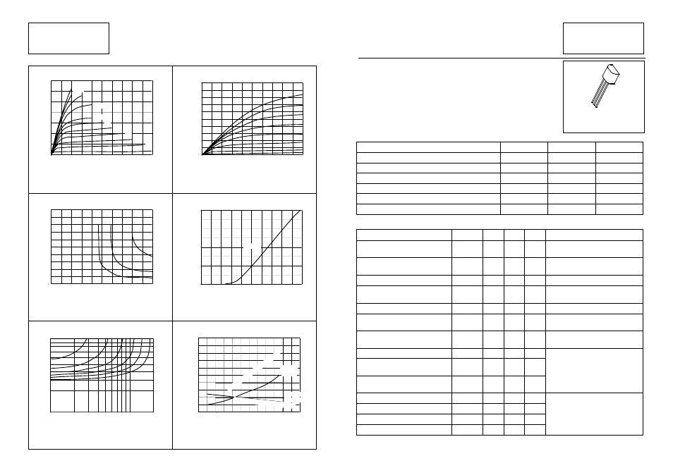
TYPICAL CHARACTERISTICS
Output Characteristics
V
DS
- Drain Source
Voltage (Volts)
I
D(
O
n
)
-On-
St
a
te
Dr
ain
Cu
rr
e
n
t (
Am
ps)
Transfer Characteristics
Normalised R
DS(on)
and V
GS(th)
vs Temperature
Normalised R
D
S
(o
n)
a
nd
V
G
S
(th)
-40 -20
0
20 40 60 80
120
100
140 160
2.4
2.2
2.0
1.8
1.6
1.4
1.2
1.0
0.6
0.8
Dr
ai
n-
So
urc
e R
es
ista
nc
e
R
DS(
on
)
Gate Threshold Vo
ltage V
GS(th)
I
D=-
0.5A
0
-2
-4
-6
-8
-10
0
-10
-20
-30
-40
-50
Saturation Characteristics
V
DS-
D
ra
in
S
ourc
e
V
olt
age (V
o
lt
s
)
Voltage Saturation Characteristics
V
GS-
Gate Source Voltage
(Volts)
-10V
I
D(
O
n
)-
On-State Drain Current (Amps)
V
GS-
Gate Source
Voltage (Volts)
V
GS=
-10V
I
D=
-1mA
V
GS=
V
DS
-3.5
-3.0
-2.0
-0.5
0
-1.0
-2.5
-1.5
2.6
180
V
GS=
-20V
-14V
-5V
-6V
-7V
-4V
-3.5V
-8V
V
GS
=
-18V
I
D(O
n
)
-On-State Drain Current (Amps)
V
DS
- Drain Source
Voltage (Volts)
On-resistance v drain current
I
D
-Drain Current
(Amps)
R
DS(ON)
-D
ra
in
So
u
rce
Re
sist
a
n
ce
(
Ω
)
-0.1
-1.0
10
5
-2.0
-12V
-6V
-4V
0
-2
-4
-6
-8
-10
1
-10V
-9V
-8V
-7V
-5V
-9V
0
-0.6
-0.4
-0.2
-0.8
-1.6
-1.4
-1.2
-1.0
-1.8
-2.0
0
-10
-6
-2
-4
-8
0
-2
-4
-6
-8
-10
I
D=
-1A
-0.5A
-0.25A
-0.8
-0.6
-0.2
-0.4
V
DS=
-10V
-1.6
-1.4
-1.0
-1.2
-6V
-7V
V
GS
=-5V
-8V
-10V
-9V
T
j
-Junction Temperature (°C)
ZVP2106A
3-418