Maximum ratings, Thermal characteristics, Electrical characteristics – Diodes ZVN4310G User Manual
Page 2: Zvn4310g, A product line of diodes incorporated
ZVN4310G
Document number: DS33372 Rev. 4 - 2
2 of 5
January 2012
© Diodes Incorporated
A Product Line of
Diodes Incorporated
ZVN4310G
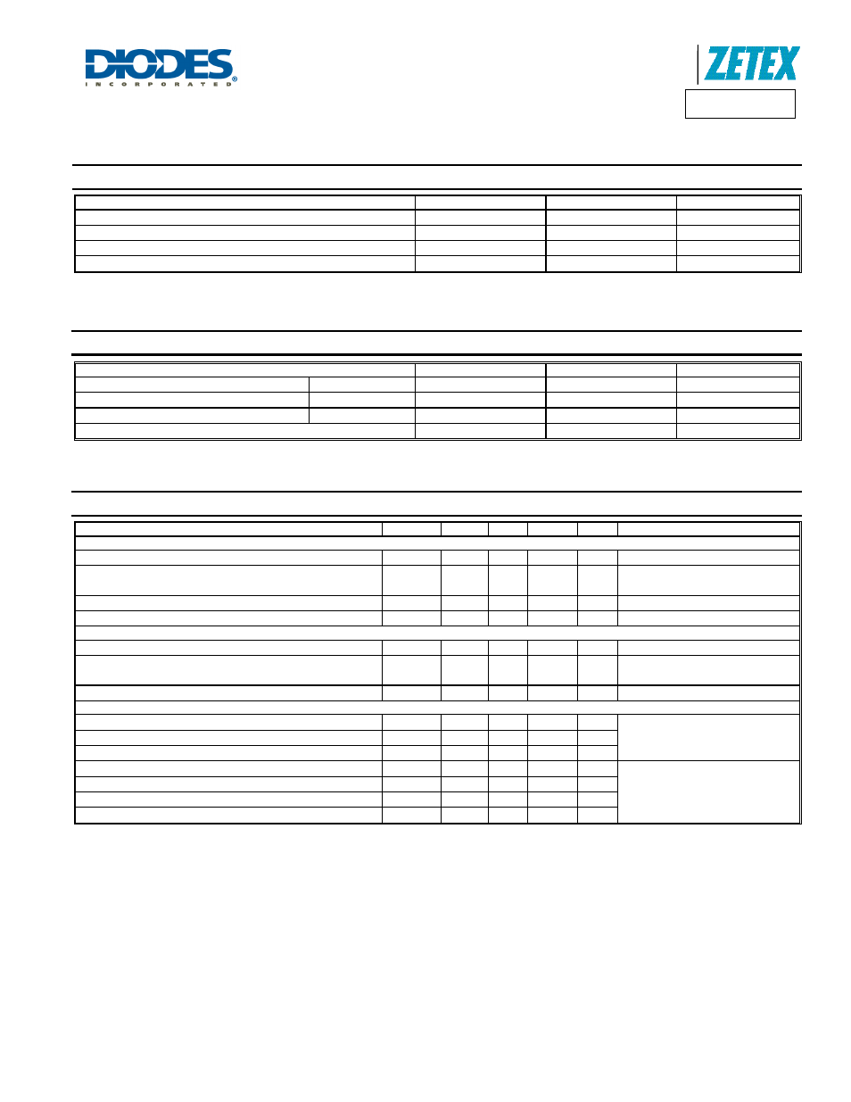
Maximum Ratings
@T
A
= 25°C unless otherwise specified
Characteristic
Symbol
Value
Unit
Drain-Source Voltage
V
DSS
100 V
Gate-Source Voltage
V
GSS
±20 V
Continuous Drain Current
I
D
1.67 A
Pulsed Drain Current (Note 3)
I
DM
12 A
Thermal Characteristics
@T
A
= 25°C unless otherwise specified
Characteristic Symbol
Value
Unit
Power Dissipation
(Note 2)
P
D
3 W
Thermal Resistance, Junction to Ambient
(Note 2)
R
θJA
41.7 °C/W
Thermal Resistance, Junction to Leads
(Note 4)
R
θJL
8.84 °C/W
Operating and Storage Temperature Range
T
J
,
T
STG
-55 to +150
°C
Electrical Characteristics
@T
A
= 25°C unless otherwise specified
Characteristic
Symbol
Min
Typ
Max
Unit
Test Condition
OFF CHARACTERISTICS (Note 5)
Drain-Source Breakdown Voltage
BV
DSS
100 - - V
V
GS
= 0V, I
D
= 1mA
Zero Gate Voltage Drain Current T
J
= 25°C
I
DSS
- -
10
100
µA
µA
V
DS
= 100V, V
GS
= 0V
V
DS
= 80V, V
GS
= 0V, T
A
= 125°C
Gate-Source Leakage
I
GSS
- -
±20
nA
V
GS
= ±20V, V
DS
= 0V
On-State Drain Current
I
D(on)
9 - - A
V
GS
= 10V, V
DS
= 10V
ON CHARACTERISTICS (Note 5)
Gate Threshold Voltage
V
GS(th)
1 - 3 V
V
DS
= V
GS
, I
D
= 1mA
Static Drain-Source On-Resistance
R
DS (on)
-
0.4
0.5
0.54
0.75
Ω
V
GS
= 10V, I
D
= 3.3A
V
GS
= 5V, I
D
= 1.5A
Forward Transconductance
g
fs
0.6 - - S
V
DS
= 10V, I
D
= 3.3A
DYNAMIC CHARACTERISTICS (Note 5)
Input Capacitance
C
iss
- -
350
pF
V
DS
= 25V, V
GS
= 0V,
f = 1.0MHz
Output Capacitance
C
oss
- -
140
pF
Reverse Transfer Capacitance
C
rss
- - 20
pF
Turn-On Delay Time
t
D(on)
- - 8 ns
V
DD
= 25V, I
D
= 3A, V
GEN
= 10V,
R
GS
= 50
Ω
Turn-On Rise Time
t
r
- - 25
ns
Turn-Off Delay Time
t
D(off)
- - 30
ns
Turn-Off Fall Time
t
f
- - 16
ns
Notes:
2. For a device mounted on 50mm X 50mm X 1.6mm FR-4 PCB with high coverage of single sided 2oz copper, in still air condition.
3. Device mounted on minimum recommended pad layout test board, 10
μs pulse duty cycle = 1%.
4. Thermal resistance from junction to solder-point (at the end of the drain lead).
5. Short duration pulse test used to minimize self-heating effect.