Diodes ZVN4310A User Manual
Zvn4310a, N-channel enhancement mode vertical dmos fet
N-CHANNEL ENHANCEMENT
MODE VERTICAL DMOS FET
ISSUE 2 – MARCH 94
FEATURES
*
100 Volt V
DS
*
R
DS(on)
= 0.5
Ω
*
Spice model available
ABSOLUTE MAXIMUM RATINGS.
PARAMETER
SYMBOL
VALUE
UNIT
Drain-Source Voltage
V
DS
100
V
Continuous Drain Current at T
amb
=25°C
I
D
0.9
A
Practical Continuous Drain Current at
T
amb
=25°C
I
DP
1
A
Pulsed Drain Current
I
DM
12
A
Gate Source Voltage
V
GS
±
20
V
Power Dissipation at T
amb
=25°C
P
tot
850
mW
Practical Power Dissipation at T
amb
=25°C*
P
totp
1.13
W
Operating and Storage Temperature Range
T
j
:T
stg
-55 to +150
°C
*The power which can be dissipated assuming the device is mounted in a typical manner on a P.C.B.
with copper equal to 1 inch square minimum
ELECTRICAL CHARACTERISTICS (at T
amb
= 25°C unless otherwise stated).
PARAMETER
SYMBOL MIN.
TYP.
MAX.
UNIT CONDITIONS.
Drain-Source
Breakdown Voltage
BV
DSS
100
V
I
D
=1mA, V
GS
=0V
Gate-Source
Threshold Voltage
V
GS(th)
1
3
V
ID=1mA, V
DS
= V
GS
Gate-Body Leakage
I
GSS
20
nA
V
GS
=
±
20V, V
DS
=0V
Zero Gate Voltage
Drain Current
I
DSS
10
100
µ
A
µ
A
V
DS
=100V, V
GS
=0
V
DS
=80V, V
GS
=0V, T=125°C
(2)
On-State Drain
Current(1)
I
D(on)
9
A
V
DS
=25 V, V
GS
=10V
Static Drain-Source
On-State Resistance
(1)
R
DS(on)
0.36
0.48
0.5
0.65
Ω
Ω
V
GS
=10V,I
D
=3A
V
GS
=5V, I
D
=1.5A
Forward
Transconductance
(1)(2)
g
fs
600
mS
V
DS
=25V,I
D
=3A
E-Line
TO92 Compatible
ZVN4310A
3-393
D
G
S
ELECTRICAL CHARACTERISTICS (at T
amb
= 25°C unless otherwise stated).
PARAMETER
SYMBOL MIN.
TYP.
MAX.
UNIT
CONDITIONS.
Input Capacitance (2)
C
iss
350
pF
Common Source
Output Capacitance
(2)
C
oss
140
pF
V
DS
=25 V, V
GS
=0V, f=1MHz
Reverse Transfer
Capacitance (2)
C
rss
30
pF
Turn-On Delay Time
(2)(3)
t
d(on)
8
ns
V
DD
≈
25V, V
GEN
=10V, I
D
=3A
R
GS
=50
Ω
Rise Time (2)(3)
t
r
25
ns
Turn-Off Delay Time
(2)(3)
t
d(off)
30
ns
Fall Time (2)(3)
t
f
16
ns
(1) Measured under pulsed conditions. Width=300
µ
s. Duty cycle
≤
2%
(2) Sample test.
(3) Switching times measured with 50
Ω
source impedance and <5ns rise time on a pulse generator
THERMAL CHARACTERISTICS
PARAMETER
SYMBOL
MAX.
UNIT
Thermal Resistance:Junction to Ambient
Junction to Case
R
th(j-amb)
R
th(j-case)
150
50
°C/W
°C/W
ZVN4310A
-40
0.50
0.25
0.0001
50
150
100
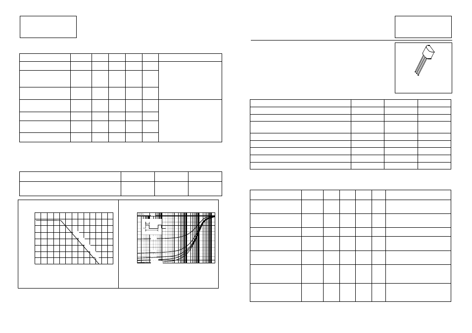
Derating curve
T
-Temperature
(°C)
Max Power Dissipation
- (W
atts)
Maximum transient thermal impedance
Pulse Width (seconds)
Thermal Resistance (°C/W)
10
100
1
0.1
0.01
1.0
0.75
-20
0
20 40
60 80 100 120
200
180
160
140
t
1
t
P
D=t
1
/t
P
Am
bie
nt t
empe
rat
ure
D.C.
D=0.6
D=0.2
D=0.1
Single Pulse
0.001
0
D=0.05
3-394