Diodes ZVN4306G User Manual
Zvn4306g, Typical characteristics
SOT223 N-CHANNEL ENHANCEMENT
MODE VERTICAL DMOS FET
ISSUE 3 - OCTOBER 1995
FEATURES
*
Very low R
DS(ON)
= .33
Ω
APPLICATIONS
*
DC - DC Converters
*
Solenoids/Relay Drivers for Automotive
PARTMARKING DETAIL -
ZVN4306
ABSOLUTE MAXIMUM RATINGS.
PARAMETER
SYMBOL
VALUE
UNIT
Drain-Source Voltage
V
DS
60
V
Continuous Drain Current at T
amb
=25°C
I
D
2.1
A
Pulsed Drain Current
I
DM
15
A
Gate Source Voltage
V
GS
±
20
V
Power Dissipation at T
amb
=25°C
P
tot
3
W
Operating and Storage Temperature Range
T
j
:T
stg
-55 to +150
°C
ELECTRICAL CHARACTERISTICS (at T
amb
= 25°C unless otherwise stated).
PARAMETER
SYMBOL MIN.
TYP.
MAX.
UNIT
CONDITIONS.
Drain-Source
Breakdown Voltage
BV
DSS
60
V
I
D
=1mA, V
GS
=0V
Gate-Source Threshold
Voltage
V
GS(th)
1.3
3
V
I
D
=1mA, V
DS
= V
GS
Gate-Body Leakage
I
GSS
20
nA
V
GS
=
±
20V, V
DS
=0V
Zero Gate Voltage
Drain Current
I
DSS
10
100
µ
A
µ
A
V
DS
=60V, V
GS
=0V
V
DS
=48V, V
GS
=0V, T=125°C
(2)
On-State Drain
Current(1)
I
D(on)
12
A
V
DS
=10V, V
GS
=10V
Static Drain-Source
On-State Resistance (1)
R
DS(on)
0.22
0.32
0.33
0.45
Ω
Ω
V
GS
=10V, I
D
=3A
V
GS
=5V, I
D
=1.5A
Forward
Transconductance (1)
g
fs
0.7
S
V
DS
=25V,I
D
=3A
Input Capacitance (2)
C
iss
350
pF
Common Source
Output Capacitance (2)
C
oss
140
pF
V
DS
=25 V, V
GS
=0V, f=1MHz
Reverse Transfer
Capacitance (2)
C
rss
30
pF
Turn-On Delay Time
(2)(3)
t
d(on)
8
ns
V
DD
≈
25V, V
GEN
=10V, I
D
=3A
Rise Time (2)(3)
t
r
25
ns
Turn-Off Delay Time
(2)(3)
t
d(off)
30
ns
Fall Time (2)(3)
t
f
16
ns
(1) Measured under pulsed conditions. Width=300
µ
s. Duty cycle
≤
2% (2) Sample test.
(3) Switching times measured with 50
Ω
source impedance and <5ns rise time on a pulse generator
Spice parameter data is available upon request for this device
ZVN4306G
D
D
S
G
3 - 412
ZVN4306G
3 - 411
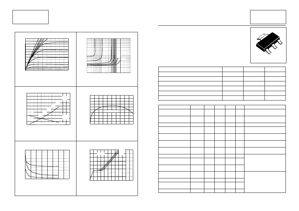
TYPICAL CHARACTERISTICS
Saturation Characteristics
V
DS
- Drain Source
Voltage (Volts)
0
1
2
3
4
5
6
7
8
9
10
I
D
- Dra
in Curr
ent
(Amps)
Normalised R
DS(on)
and V
GS(th)
v Temperature
T
j
-Junction Temperature (°C)
N
o
rm
al
ised
R
D
S(
on
)
and
V
G
S(t
h)
-50 -25
0
25 50 75 100
150
125
175 200
2.4
2.2
2.0
1.8
1.6
1.4
1.2
1.0
0.6
0.8
Dr
ai
n-S
our
ce
Res
ist
anc
e
R
DS(on)
Gate Threshold Voltage V
GS(TH)
I
D=
3A
V
GS=
10V
I
D=
1mA
V
GS=
V
DS
2.6
225
0
4
1
2
7
6
5
3
10
9
8
10V
8V
9V
7V
5V
4V
6V
3.5V
V
GS=
20V 12V
On-resistance v drain current
I
D-
Drain Current
(Amps)
R
D
S
(on
)
-Drai
n Source On Resi
stance
(
Ω
)
0.1
10
100
3.5V
5V
V
GS
=3V
6V
0.1
10
1.0
1
10V
3V
12
11
V
DS
-Drain Source Voltage (Volts)
Capacitance v drain-source voltage
C
-C
ap
aci
tance
(pF)
C
oss
C
iss
C
rss
0
10
20
30
40
50
60
70
80
0
300
200
100
400
500
Q-Charge (nC)
V
GS
-Gat
e
Source
V
o
lt
age
(V
ol
ts)
Gate charge v gate-source voltage
0
10
8
6
2
0
4
12
14
16
V
DD
=
20V
I
D=
3A
40V
60V
1
2
3
4
5
6
7
8
9
10 11 12
Transconductance v drain current
I
D(on)
- Drain Current (Amps
)
g
fs
-T
ranscon
ductan
c
e
(S)
0
2
4
6
8
10
V
DS=
10V
0
1
2
4
3
5
12
14
16
18
20
8V