Diodes ZVN3306A User Manual
Zvn3306a, N-channel enhancement mode vertical dmos fet, Typical characteristics
N-CHANNEL ENHANCEMENT
MODE VERTICAL DMOS FET
ISSUE 2 – MARCH 94
FEATURES
*
60 Volt V
DS
*
R
DSon)
=5
Ω
ABSOLUTE MAXIMUM RATINGS.
PARAMETER
SYMBOL
VALUE
UNIT
Drain-Source Voltage
V
DS
60
V
Continuous Drain Current at T
amb
=25°C
I
D
270
mA
Pulsed Drain Current
I
DM
3
A
Gate-Source Voltage
V
GS
±
20
V
Power Dissipation at T
amb
=25°C
P
tot
625
mW
Operating and Storage Temperature Range
T
j
:T
stg
-55 to +150
°C
ELECTRICAL CHARACTERISTICS (at T
amb
= 25°C unless otherwise stated).
PARAMETER
SYMBOL MIN.
MAX. UNIT CONDITIONS.
Drain-Source Breakdown
Voltage
BV
DSS
60
V
I
D
=1mA, V
GS
=0V
Gate-Source Threshold
Voltage
V
GS(th)
0.8
2.4
V
ID=1mA, V
DS
= V
GS
Gate-Body Leakage
I
GSS
20
nA
V
GS
=
±
20V, V
DS
=0V
Zero Gate Voltage Drain
Current
I
DSS
0.5
50
µ
A
µ
A
V
DS
=60V, V
GS
=0
V
DS
=48V, V
GS
=0V, T=125°C
(2)
On-State Drain Current(1)
I
D(on)
750
mA
V
DS
=18V, V
GS
=10V
Static Drain-Source On-State
Resistance (1)
R
DS(on)
5
Ω
V
GS
=10V,I
D
=500mA
Forward Transconductance(1)(2
)
g
fs
150
mS
V
DS
=18V,I
D
=500mA
Input Capacitance (2)
C
iss
35
pF
Common Source Output
Capacitance (2)
C
oss
25
pF
V
DS
=18V, V
GS
=0V, f=1MHz
Reverse Transfer Capacitance
(2)
C
rss
8
pF
Turn-On Delay Time (2)(3)
t
d(on)
5
ns
V
DD
≈
18V, I
D
=500mA
Rise Time (2)(3)
t
r
7
ns
Turn-Off Delay Time (2)(3)
t
d(off)
6
ns
Fall Time (2)(3)
t
f
8
ns
(1) Measured under pulsed conditions. Width=300
µ
s. Duty cycle
≤
2%
(
2) Sample test.
E-Line
TO92 Compatible
ZVN3306A
3-375
D
G
S
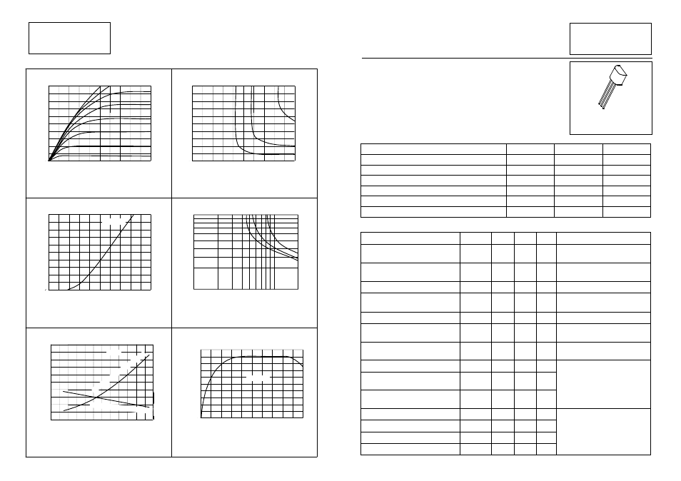
TYPICAL CHARACTERISTICS
V
DS
- Drain Source
Voltage (Volts)
I
D(O
n
)
-On-State Drain Curren
t (Amps)
Transfer Characteristics
Saturation Characteristics
V
DS-
Drain Source
V
oltage (V
olts)
Voltage Saturation Characteristics
V
GS-
Gate Source Voltage
(Volts)
I
D=
1A
0.5A
0.25A
I
D(
O
n
)
-On-
S
tat
e
Drain Cur
re
n
t (
Am
ps)
V
GS
-Gate Source
Voltage (Volts)
0.6
0
0.2
0.4
0.8
0
2
4
6
8
10
1.0
V
GS=
10V
5V
7V
8V
6V
4V
3V
9V
Normalised R
DS(on)
and V
GS(th)
vs Temperature
Nor
m
ali
s
e
d
R
DS(on)
a
nd V
G
S(
th
)
-40 -20
0 20 40 60 80
120
100
140 160
2.4
2.2
2.0
1.8
1.6
1.4
1.2
1.0
0.6
0.8
Dr
ai
n-S
ou
rc
e R
es
ista
nc
e
R
DS(
on
)
Gate Threshold Vo
ltage V
GS(th)
I
D=-
0.5A
T-Temperature (C°)
0.4
-80 -60
0.6
0
0.2
0.4
0.8
0
2
4
6
8
10
1.0
6
0
2
4
8
0
2
4
6
8
10
10
On-resistance vs gate-source voltage
V
GS
-Gate Source Voltage
(Volts)
R
DS
(O
N)
-D
ra
in So
urc
e
Res
is
ta
n
c
e
(
Ω
)
1
10
20
1
10
5
Transconductance v drain current
I
D(on)
- Drain Current (Amps
)
g
fs
-Fo
rwar
d
T
ra
nsc
o
ndu
cta
nce (mS)
0
0.1 0.2
0.3
0.4
0.5
0.6
0.7 0.8
0.9
1.0
0
V
DS=
18V
60
40
20
80
160
140
120
100
180
200
V
DS=
10V
I
D=
1A
0.5A
0.25A
ZVN3306A
3-376