Package outline dimensions, Suggested pad layout – Diodes ZXTN04120HK User Manual
Page 6
ZXTN04120HK
Document number: DS36554 Rev. 3 - 2
6 of 7
January 2014
© Diodes Incorporated
A Product Line of
Diodes Incorporated
ZXTN04120HK
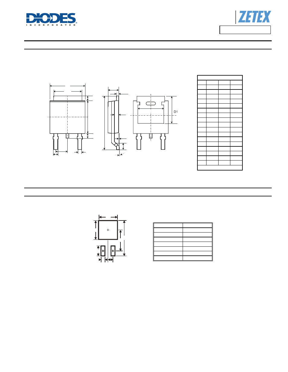
Package Outline Dimensions
rsion.
Suggested Pad Layout
e latest version.
Note:
12. For high voltage applications, the appropriate industry sector guidelines should be considered with regards to creepage and clearance distances
between device Terminals and PCB tracking.
TO252
Dim Min Max Typ
A
2.19 2.39 2.29
A1 0.00 0.13 0.08
A2 0.97 1.17 1.07
b
0.64 0.88 0.783
b2 0.76 1.14 0.95
b3 5.21 5.46 5.33
c2 0.45 0.58 0.531
D
6.00 6.20 6.10
D1 5.21
e
2.286
E
6.45 6.70 6.58
E1 4.32
H
9.40 10.41 9.91
L
1.40 1.78 1.59
L3 0.88 1.27 1.08
L4 0.64 1.02 0.83
a
0° 10°
All Dimensions in mm
Dimensions
Value (in mm)
Z
11.6
X1
1.5
X2
7.0
Y1
2.5
Y2
7.0
C
6.9
E1
2.3
b3
E
2X b2
D
L4
A
c2
e
A1
L
L3
3X b
a
H
A2
E1
X2
C
Z
X1
Y1
E1
Y2
- PDS3200 (5 pages)
- PDS340 (5 pages)
- PDS340Q (5 pages)
- PDS360 (5 pages)
- PDS360Q (5 pages)
- PDS4150 (4 pages)
- PDS3100Q (5 pages)
- PDS3100 (5 pages)
- PDS1240CTL (5 pages)
- PDS1045 (5 pages)
- PDS1040L (5 pages)
- PDS1040CTL (5 pages)
- PDS1040 (5 pages)
- PD3S230L (5 pages)
- PD3S230H (3 pages)
- PDS5100Q (5 pages)
- PDS835L (5 pages)
- PDS760 (5 pages)
- PDS560 (5 pages)
- PDS540 (5 pages)
- PDS5100H (5 pages)
- PDS5100 (5 pages)
- PDS4200H (6 pages)
- SBL3060CTP (4 pages)
- SBL30L30CT (3 pages)
- SBL3045CTP (4 pages)
- SBL3040CTP (4 pages)
- SBL2060CTP (4 pages)
- SBL2030CT - SBL2060CT (3 pages)
- SBL2045CTP (4 pages)
- SBL1060CTP (4 pages)
- SBL1040CTP (4 pages)
- SBG3030CT - SBG3045CT (5 pages)
- SB520 - SB560 (3 pages)
- SB370 - SB3100 (3 pages)
- SB320 - SB360 (3 pages)
- SBR10U100CT (5 pages)
- SBR10U150CT (5 pages)
- SBR10A45SP5 (5 pages)
- SBR1060CT (5 pages)
- SBR1045SP5 (5 pages)
- SBR1045SD1 (4 pages)
- SBR1045D1 (5 pages)
- SBR1045CTL (4 pages)
- SBR1040CT (5 pages)