Diodes UMG4N User Manual
Umg4n, Features, Mechanical data
UMG4N
DS31207 Rev. 3 - 2
1 of 3
www.diodes.com
UMG4N
© Diodes Incorporated
DUAL NPN PRE-BIASED TRANSISTOR
Features
•
Epitaxial Planar Die Construction
•
Surface Mount Package Suited for Automated Assembly
•
Simplifies Circuit Design and Reduces Board Space
•
Lead Free/RoHS Compliant (Note 1)
•
"Green" Device (Note 2)
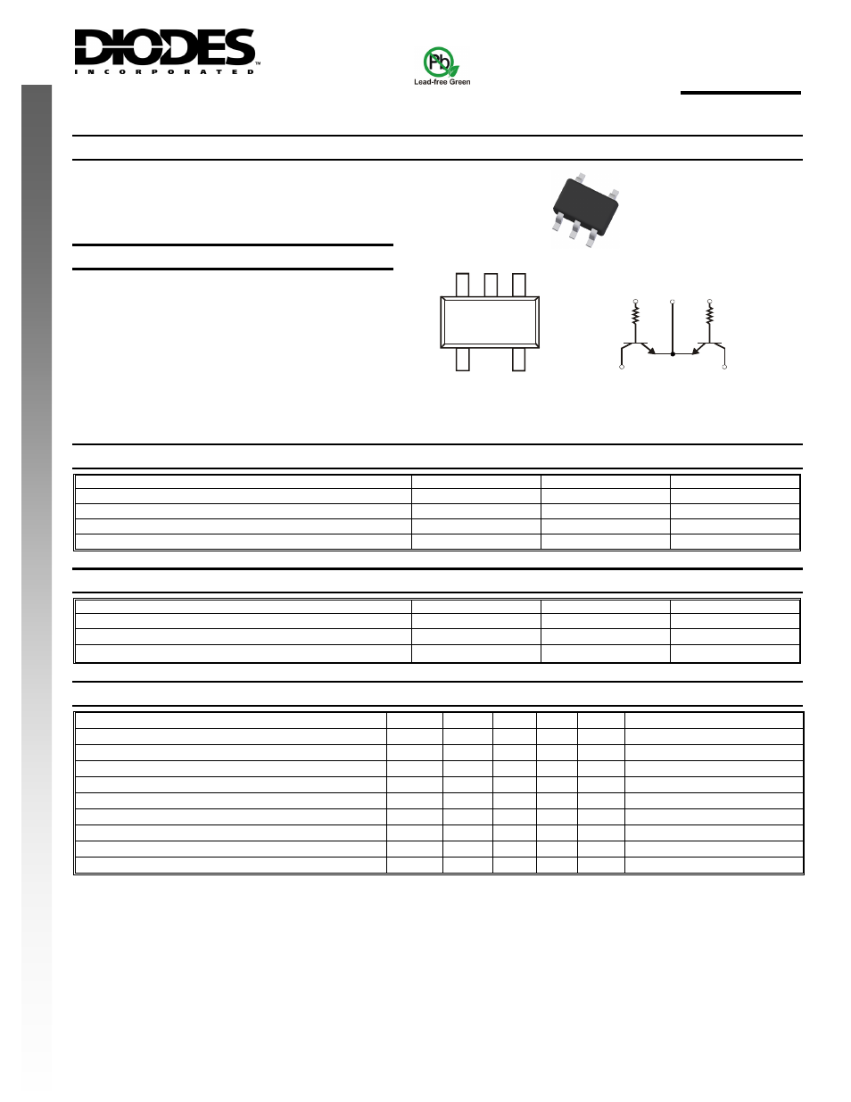
Mechanical Data
•
Case: SOT-353
•
Case Material: Molded Plastic. UL Flammability
Classification Rating 94V-0
•
Moisture Sensitivity: Level 1 per J-STD-020C
•
Terminal Connections: See Diagram
•
Terminals: Finish – Matte Tin Annealed Over Alloy 42
Leadframe. Solderable per MIL-STD-202, Method 208
•
Marking Information: See Page 2
•
Ordering Information: See Page 2
•
Weight: 0.006 grams (approximate)
NEW PROD
UC
T
SOT-353
3
2
1
4
5
TOP VIEW
R1
(3)
(2)
(1)
(4)
(5)
R1
Schematic and Pin Configuration
Maximum Ratings
@T
A
= 25°C unless otherwise specified
Characteristic Symbol
Value
Unit
Collector-Base Voltage
V
CBO
50 V
Collector-Emitter Voltage
V
CEO
50 V
Emitter-Base Voltage
V
EBO
5 V
Collector Current
I
C
100 mA
Thermal Characteristics
Characteristic Symbol
Value
Unit
P
D
150 mW
Power Dissipation @T
A
= 25°C (Note 3)
R
θJA
833
°C/W
Thermal Resistance, Junction to Ambient Air @T
A
= 25°C (Note 3)
Operating and Storage Temperature Range
T
j
, T
STG
-55 to +150
°C
Electrical Characteristics
@T
A
= 25°C unless otherwise specified
Characteristic Symbol
Min
Typ
Max
Unit
Test
Condition
Collector-Base Breakdown Voltage
V
(BR)CBO
50
⎯
⎯
V
I
C
= 50
μA, I
E
= 0
Collector-Emitter Breakdown Voltage
V
(BR)CEO
50
⎯
⎯
V
I
C
= 1mA, I
B
= 0
Emitter-Base Breakdown Voltage
V
(BR)EBO
5.0
⎯
⎯
V
I
E
= 50
μA, I
C
= 0
Collector Cut-Off Current
I
CBO
⎯
⎯
0.5
μA
V
CB
= 50V, I
E
= 0
Emitter Cut-Off Current
I
EBO
⎯
⎯
0.5
μA
V
EB
= 4V, I
C
= 0
Collector-Emitter Saturation Voltage
V
CE(SAT)
⎯
⎯
0.3 V
I
C
= 10mA, I
B
= 1mA
DC Current Gain
h
FE
100 330 600
⎯
V
CE
= 5V, I
C
= 1mA
Gain-Bandwidth Product (Note 4)
f
T
⎯
250
⎯
MHz V
CE
= 10V, I
E
= -5mA, f = 100MHz
Input Resistance
R
1
7 10
13
k
Ω
⎯
Notes:
1. No purposefully added lead.
2. Diodes Inc.'s "Green" policy can be found on our website at http://www.diodes.com/products/lead_free/index.php.
3. Device mounted on FR-4 PCB; pad layout as shown on Diodes Inc. suggested pad layout document AP02001, which can be found on our website at
http://www.diodes.com/datasheets/ap02001.pdf.
4. Characteristics of transistor. For reference only.