Diodes ZTX694B User Manual
Ztx694b
NPN SILICON PLANAR MEDIUM POWER
HIGH GAIN TRANSISTOR
ISSUE 1 APRIl 94
FEATURES
* 120 Volt V
CEO
* Gain of 400 at I
C
=200mA
* Very low saturation voltage
APPLICATIONS
* Darlington replacement
* Relay / solenoid driver
* Battery powered circuits
* Motor drivers
ABSOLUTE MAXIMUM RATINGS.
PARAMETER
SYMBOL
VALUE
UNIT
Collector-Base Voltage
V
CBO
120
V
Collector-Emitter Voltage
V
CEO
120
V
Emitter-Base Voltage
V
EBO
5
V
Peak Pulse Current
I
CM
1
A
Continuous Collector Current
I
C
0.5
A
Practical Power Dissipation*
P
totp
1.5
W
Power Dissipation T
amb
=25°C
derate above 25°C
P
tot
1
5.7
W
mW/°C
Operating and Storage Temperature Range
T
j
:T
stg
-55 to +200
°C
*The power which can be dissipated assuming the device is mounted in a typical manner on a
P.C.B. with copper equal to 1 inch square minimum
ELECTRICAL CHARACTERISTICS (at T
amb
= 25°C)
PARAMETER
SYMBOL
MIN.
TYP.
MAX. UNIT CONDITIONS.
Collector-Base Breakdown
Voltage
V
(BR)CBO
120
V
I
C
=100
µ
A
Collector-Emitter Breakdown
Voltage
V
(BR)CEO
120
V
I
C
=10mA*
Emitter-Base Breakdown
Voltage
V
(BR)EBO
5
V
I
E
=100
µ
A
Collector Cut-Off Current
I
CBO
0.1
µ
A
V
CB
=100V
Emitter Cut-Off Current
I
EBO
0.1
µ
A
V
EB
=4V
Collector-Emitter Saturation
Voltage
V
CE(sat)
0.25
0.5
V
V
I
C
=100mA, I
B
=0.5mA*
I
C
=400mA, I
B
=5mA*
Base-Emitter
Saturation Voltage
V
BE(sat)
0.9
V
I
C
=1A, I
B
=10mA*
Base-Emitter
Turn-On Voltage
V
BE(on)
0.9
V
IC=1A, V
CE
=2V*
Static Forward Current
Transfer Ratio
h
FE
500
400
150
I
C
=100mA, V
CE
=2V
*
I
C
=200mA, V
CE
=2V*
I
C
=400mA, V
CE
=2V*
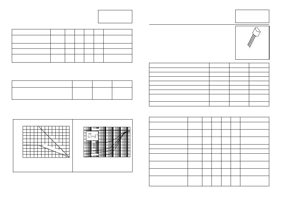
E-Line
TO92 Compatible
ZTX694B
3-244
C
B
E
ELECTRICAL CHARACTERISTICS (at T
amb
= 25°C)
PARAMETER
SYMBOL
MIN.
TYP.
MAX. UNIT CONDITIONS.
Transition Frequency
f
T
130
MHz
I
C
=50mA, V
CE
=5V
f=50MHz
Input Capacitance
C
ibo
200
pF
V
EB
=0.5V, f=1MHz
Output Capacitance
C
obo
9
pF
V
CB
=10V, f=1MHz
Switching Times
t
on
t
off
80
2900
ns
ns
I
C
=100mA, I
B!
=10mA
I
B2
=10mA, V
CC
=50V
*Measured under pulsed conditions. Pulse width=300
µ
s. Duty cycle
≤
2%
THERMAL CHARACTERISTICS
PARAMETER
SYMBOL
MAX.
UNIT
Thermal Resistance:Junction to Ambient
1
Junction to Ambient
2
Junction to Case
R
th(j-amb)1
R
th(j-amb)2
R
th(j-case)
175
116
70
°C/W
°C/W
°C/W
Device mounted on P.C.B. with copper equal to 1 sq. Inch minimum.
ZTX694B
-40
0.0001
Derating curve
T
-Temperature
(°C)
M
ax Po
we
r D
is
sipat
io
n
- (
W
a
tts)
Maximum transient thermal impedance
Pulse Width (seconds)
T
h
e
rm
a
l R
esis
ta
nce (
°C/
W
)
10
100
1
0.1
0.01
-20
0
20 40
60 80 100 120
200
180
160
140
0.001
0
100
200
D=0.2
D=0.1
Single Pulse
D=0.5
t
1
t
P
D=t
1
/t
P
1.0
0.5
2.0
1.5
Case temperature
2.5
Ambient temperat
ure
0
D=1 (D.C.)
3-245