Zxtn618ma, Maximum ratings, Thermal characteristics – Diodes ZXTN618MA User Manual
Page 2
ZXTN618MA
Document Number DS31890 Rev. 5 – 2
2 of 7
January 2011
© Diodes Incorporated
A Product Line of
Diodes Incorporated
ZXTN618MA
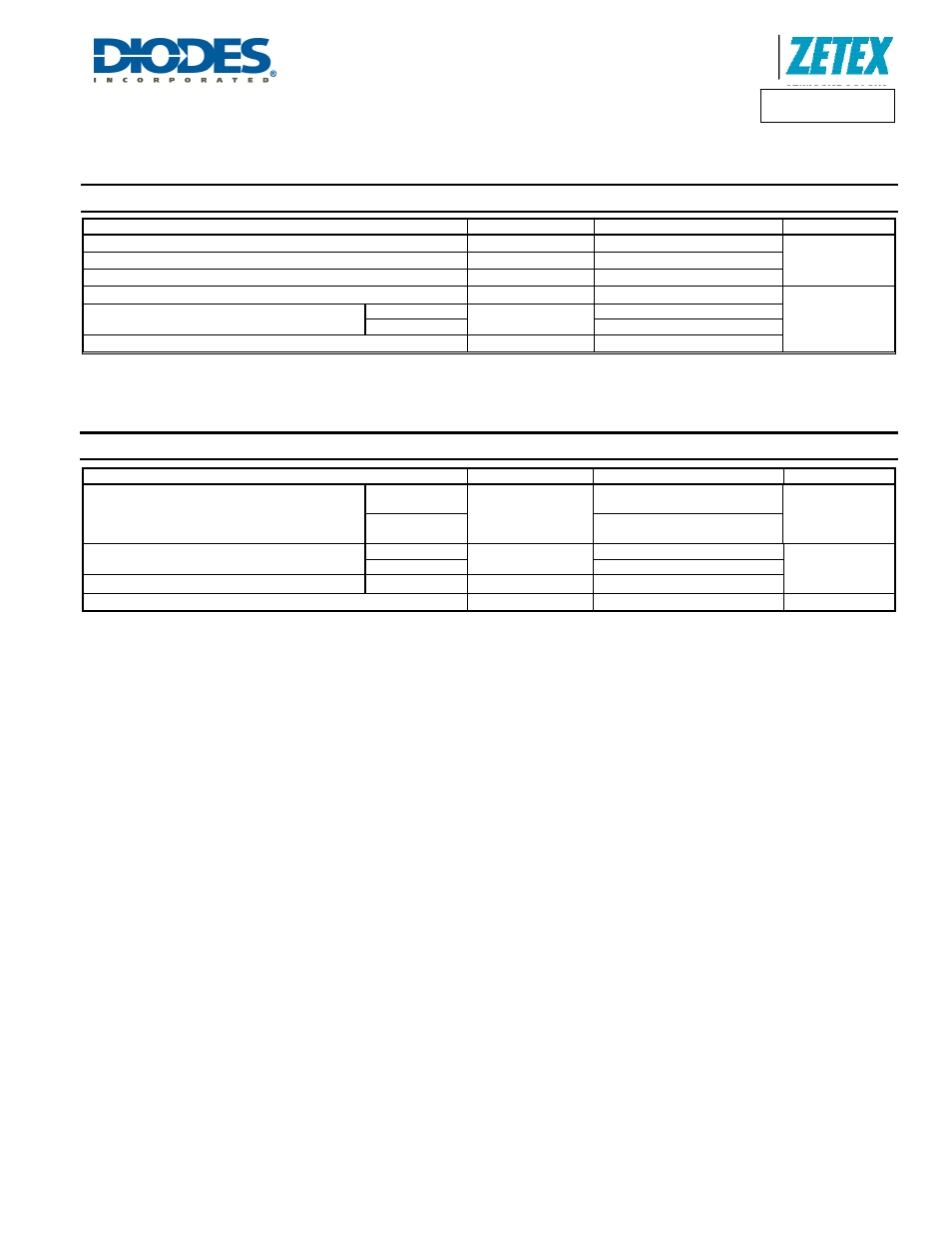
Maximum Ratings
@T
A
= 25°C unless otherwise specified
Parameter Symbol
Limit
Unit
Collector-Base Voltage
V
CBO
40
V
Collector-Emitter Voltage
V
CEO
20
Emitter-Base Voltage
V
EBO
7
Peak Pulse Current
I
CM
12
A
Continuous Collector Current
(Note 3)
I
C
4.5
(Note 4)
5
Base Current
I
B
1
Thermal Characteristics
@T
A
= 25°C unless otherwise specified
Characteristic Symbol
Value
Unit
Power Dissipation
Linear Derating Factor
(Note 3)
P
D
1.5
12
W
mW/
°C
(Note 4)
2.45
19.6
Thermal Resistance, Junction to Ambient
(Note 3)
R
θJA
83
°C/W
(Note 4)
51
Thermal Resistance, Junction to Lead
(Note 5)
R
θJL
16.8
Operating and Storage Temperature Range
T
J,
T
STG
-55 to +150
°C
Notes:
3. For a device surface mounted on 31mm x 31mm (10cm
2
) FR4 PCB with high coverage of single sided 1oz copper, in still air conditions; the device is
measured when operating in a steady-state condition. The entire exposed collector pad is attached to the heatsink.
4. Same as note (3), except the device is measured at t
≤ 5 sec.
5. For a single device, thermal resistance from junction to solder-point (at the end of the drain lead).