Diodes QZX563C6V8C User Manual
Features, Mechanical data, Maximum ratings
QZX563C6V8C
Features
•
Quad TVS in Common Anode Configuration
•
Nominal Zener Voltage: 6.8V
•
Ultra-Small Surface Mount Package
•
Ideal For Transient Suppression
•
Lead Free By Design/RoHS Compliant (Note 1)
•
"Green Device" (Note 2)
•
Qualified to AEC-Q101 Standards for High Reliability
ESD Capability
•
IEC 61000-4-2 Contact Method: ±8kV
•
IEC 61000-4-2 Air Discharge Method: ± 25kV
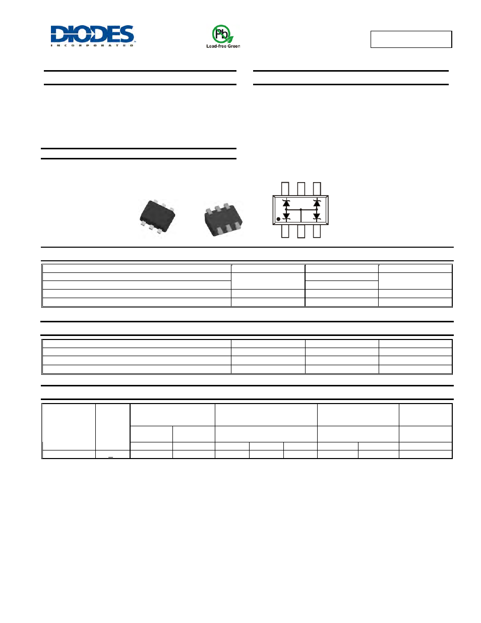
Mechanical Data
•
Case: SOT-563
•
Case Material: Molded Plastic. UL Flammability Classification
Rating 94V-0
•
Moisture Sensitivity: Level 1 per J-STD-020D
•
Terminal Finish: Matte Tin, Annealed Over Copper Leadframe.
Solderable per MIL-STD-202, Method 208
•
Orientation: See Diagram
•
Marking Information: See Page 3
•
Ordering Information: See Page 3
•
Weight: 0.003 grams (approximate)
Bottom View
Device Schematic
C
2
C
1
NC
A
C
3
C
4
Top View
Maximum Ratings
@T
A
= 25°C unless otherwise specified
Characteristic
Symbol
Value
Unit
Peak Power Dissipation, 10x1000
μS Waveform (Note 5)
10
Peak Power Dissipation, 8x20
μS Waveform (Note 5)
P
pk
80
W
Forward Voltage @ I
F
= 10mA (Note 3)
V
F
0.9
V
Forward Voltage @ I
F
= 100mA (Note 3)
V
F
1.0 V
Thermal Characteristics
Characteristic
Symbol
Value
Unit
Power Dissipation (Note 4)
P
D
150
mW
Thermal Resistance, Junction-to-Ambient (Note 4)
R
θJA
833
°C/W
Operating and Storage Temperature Range
T
J,
T
STG
-65 to +150
°C
Electrical Characteristics
@T
A
= 25°C unless otherwise specified
Reverse Standoff Voltage
and Leakage
Breakdown Voltage
(Note 3)
Maximum Reverse
Current
(Note 3)
Typical Junction
Capacitance
V
RWM
I
R
@ V
RWM
V
BR
@ I
T
= 1mA
I
R
@ V
R
C
T
@ V
R
= 0V,
f = 1MHz
Type
Number
Marking
Code
V
μA
Min (V)
Nom (V)
Max (V)
μA
V
pF
QZX563C6V8C
CB 5 1.5
6.47
6.8
7.14
1.0 3.0
63
Notes:
1. No purposefully added lead.
2. Diodes Inc.'s "Green" policy can be found on our website at http://www.diodes.com/products/lead_free/index.php.
3. Short duration pulse test used to minimize self-heating effect.
4. Device mounted on FR-4 PCB, 1 inch x 0.85 inch x 0.062 inch; pad layout as shown on Diodes Inc. Suggested Pad Layout Document AP02001,
which can be found on our website at http://www.diodes.com/datasheets/ap02001.pdf.
5. Non-repetitive current pulse per Figure 2 & 3 and derate above T
A
= 25°C per Figure 1.
QZX563C6V8C
Document number: DS30716 Rev. 4 - 2
1 of 3
www.diodes.com
July 2008
© Diodes Incorporated