Qsbt40, Maximum ratings, Thermal characteristics – Diodes QSBT40 User Manual
Page 2: Electrical characteristics
QSBT40
Document number: DS30195 Rev. 16 - 2
2 of 4
September 2012
© Diodes Incorporated
QSBT40
Maximum Ratings
(@T
A
= +25°C, unless otherwise specified.)
Single phase, half wave, 60Hz, resistive or inductive load.
For capacitance load, derate current by 20%.
Characteristic Symbol
Value
Unit
Peak Repetitive Reverse Voltage
Working Peak Reverse Voltage
DC Blocking Voltage
V
RRM
V
RWM
V
R
30 V
Forward Continuous Current (Note 6)
I
FM
200 mA
Non-Repetitive Peak Forward Surge Current @ t < 1.0s
I
FSM
600 mA
Thermal Characteristics
Characteristic Symbol
Value
Unit
Power Dissipation (Note 6)
P
D
200 mW
Thermal Resistance Junction to Ambient Air (Note 6)
R
θJA
625
°C/W
Operating Temperature Range
T
J
-55 to +125
°C
Storage Temperature Range
T
STG
-65 to +125
°C
Electrical Characteristics
(@T
A
= +25°C, unless otherwise specified.)
Characteristic Symbol
Min
Typ Max Unit
Test
Condition
Reverse Breakdown Voltage (Note 7)
V
(BR)R
30
⎯
⎯
V
I
R
= 100
μA
Forward Voltage
V
F
⎯
⎯
280
350
450
550
1000
mV
I
F
= 0.1mA, tp < 300µS
I
F
= 1.0mA, tp < 300µS
I
F
= 10mA, tp < 300µS
I
F
= 30mA, tp < 300µS
I
F
= 100mA, tp < 300µS
Reverse Current (Note 7)
I
R
⎯
⎯
2
μA
V
R
= 25V
Total Capacitance
C
T
⎯
10.0
6.5
⎯
pF
V
R
= 0, f = 1.0MHz (Note 8)
V
R
= 0, f = 1.0MH
Z
(Note 9)
Reverse Recovery Time
t
rr
⎯
⎯
5.0 ns
I
F
= I
R
= 10mA,
I
rr
= 0.1 x I
R
, R
L
= 100
Ω
Notes:
6. Device mounted on FR-4 PCB, 1 inch x 0.85 inch x 0.062 inch; pad layout as shown on Diodes Inc. suggested pad layout document AP02001, which
can be found on our website at7. Short duration pulse test used to minimize self-heating effect.
8. At V
R
= 0V, DL(X) to V
CC
or GND.
9. At V
R
= 0V, between Data Lines (e.g., DL1 and DL4).
0
50
25
50
75
100
125
150
175
200
P
,
P
O
WE
R
DISS
IP
A
T
IO
N (
m
W
)
D
T , AMBIENT TEMPERATURE (°C)
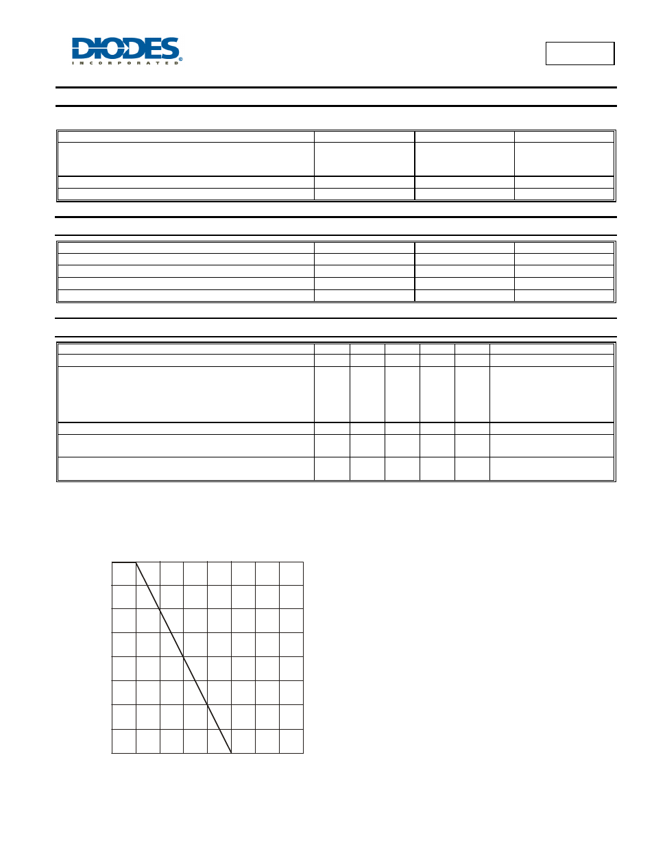
Fig. 1 Max Power Dissipation vs. Ambient Temperature
A
100
150
200
0