S1a/b - s1m/b, Maximum ratings, Thermal characteristics – Diodes S1A/B - S1M/B User Manual
Page 2: Electrical characteristics
S1A/B - S1M/B
Document number: DS16003 Rev. 23 - 2
2 of 5
March 2014
© Diodes Incorporated
S1A/B - S1M/B
Maximum Ratings
(@T
A
= +25°C, unless otherwise specified.)
Single phase, half wave, 60Hz, resistive or inductive load.
For capacitance load, derate current by 20%.
Characteristic Symbol
S1
A/AB
S1
B/BB
S1
D/DB
S1
G/GB
S1
J/JB
S1
K/KB
S1
M/MB
Unit
Peak Repetitive Reverse Voltage
Working Peak Reverse Voltage
DC Blocking Voltage
V
RRM
V
RWM
V
R
50 100 200 400 600 800 1000 V
RMS Reverse Voltage
V
R(RMS)
35 70 140 280 420 560 700 V
Average Rectified Output Current
@ T
T
= +100°C
I
O
1.0 A
Non-Repetitive Peak Forward Surge Current
8.3ms Single half sine-wave superimposed on rated load
I
FSM
30 A
Thermal Characteristics
Characteristic Symbol
Value
Unit
Typical Thermal Resistance, Junction to Terminal (Note 5)
R
θJT
30
C/W
Operating and Storage Temperature Range
T
J,
T
STG
-65 to +150
C
Electrical Characteristics
(@T
A
= +25°C, unless otherwise specified.)
Characteristic Symbol
Min
Typ
Max
Unit
Forward Voltage @ I
F
= 1.0A
V
FM
— — 1.1 V
Peak Reverse Leakage Current
@ T
A
= +25°C
at Rated DC Blocking Voltage
@ T
A
= +125°C
I
RM
—
—
—
—
5.0
100
μA
Reverse Recovery Time (Note 6)
t
rr
— 1.8 3.0
μs
Typical Total Capacitance (Note 7)
C
T
— 10 —
pF
Notes:
5. Thermal resistance junction to terminal, unit mounted on PC board with 5.0 mm
2
(0.013 mm thick) copper pads as heat sink.
6. Measured with I
F
= 0.5A, I
R
= 1.0A, I
RR
= 0.25A.
7. Measured at 1.0MHz and applied reverse voltage of 4.0V DC.
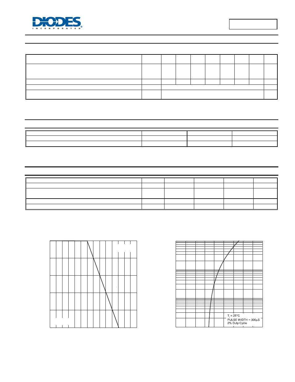
0
0.2
0.4
0.6
0.8
1.0
40
60
80
100
120
140
160
180
T , TERMINAL TEMPERATURE ( C)
Fig. 1 Forward Current Derating Curve
T
°
I,
A
V
E
R
A
G
E F
O
R
WA
R
D
C
U
R
R
E
N
T
(A
)
F
Resistive or
inductive load
0.4
0.8
0.01
0.1
10
V , INSTANTANEOUS FORWARD VOLTAGE (V)
Fig. 2 Typical Forward Characteristics
F
I
, IN
S
TAN
TANE
O
U
S F
O
R
WA
R
D
C
U
R
R
EN
T
(A
)
F
1.0
0
1.6
1.2
Note 5