Maximum ratings, Thermal characteristics, Electrical characteristics – Diodes SBR3A40SA User Manual
Page 2: Sbr3a40sa
SBR3A40SA
Document number: DS31107 Rev. 11 - 2
2 of 5
September 2013
© Diodes Incorporated
SBR3A40SA
SBR is a registered trademark of Diodes Incorporated.
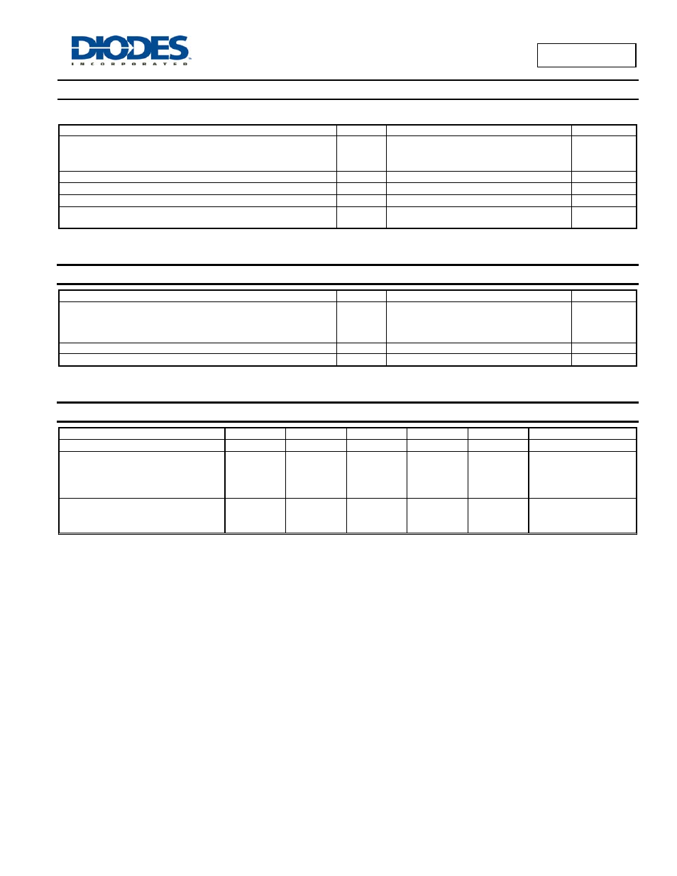
Maximum Ratings
(@T
A
= +25°C, unless otherwise specified.)
Single phase, half wave, 60Hz, resistive or inductive load
For capacitance load, derate current by 20%.
Characteristic Symbol
Value
Unit
Peak Repetitive Reverse Voltage
Working Peak Reverse Voltage
DC Blocking Voltage
V
RRM
V
RWM
V
RM
40 V
Maximum Voltage Rate of Change (Rated V
R
)
dv/dt 10,000
V/
μs
RMS Reverse Voltage
V
R(RMS)
28 V
Average Rectified Output Current
I
O
3 A
Non-Repetitive Peak Forward Surge Current 8.3ms
Single Half Sine-Wave Superimposed on Rated Load
I
FSM
45 A
Thermal Characteristics
Characteristic Symbol
Value
Unit
Maximum Thermal Resistance
Thermal Resistance Junction to Soldering (Note 7)
Thermal Resistance Junction to Ambient (Note 8)
Thermal Resistance Junction to Case (Note 8)
R
JS
R
JA
R
JC
5
124
14.3
°C/W
Power Dissipation (Note 8) @T
A
= +25°C
P
D
1.2
W
Operating and Storage Temperature Range
T
J
, T
STG
-65 to +150
°C
Electrical Characteristics
(@T
A
= +25°C, unless otherwise specified.)
Characteristic Symbol
Min
Typ
Max
Unit
Test
Condition
Reverse Breakdown Voltage (Note 10)
V
(BR)R
40 – – V
I
R
= 0.4mA
Forward Voltage Drop
V
F
–
–
–
0.30
0.33
0.43
–
0.35
0.38
0.50
0.48
V
I
F
= 0.5A, T
J
= +25°C
I
F
= 1.0A, T
J
= +25°C
I
F
= 3.0A, T
J
= +25°C
I
F
= 3.0A, T
J
= +125°C
Leakage Current (Note 10)
I
R
–
45
80
9
250
400
40
μA
μA
mA
V
R
= 5V, T
J
= +25°C
V
R
= 40V, T
J
= +25°C
V
R
= 40V, T
J
= +125°C
Notes:
7. Theoretical R
JS
calculated from the top center of the die straight down to the PCB cathode tab solder junction.
8. FR-4 PCB, 2 oz. Copper, minimum recommended pad lay9. Polymide PCB, 2 oz. Copper, minimum recommended pad layout pe10. Short duration pulse test used to minimize self-heating effect.
11. FR-4 PCB, 2 oz. Copper, single side 16 x MRP, 1” x 1” PC Board.