Diodes SBR05M100BLP User Manual
Features, Mechanical data, Maximum ratings
SBR05M100BLP
Document number: DS31109 Rev. 8 - 2
1 of 4
June 2010
© Diodes Incorporated
SBR05M100BLP
SBR is a registered trademark of Diodes Incorporated.
0.5A SBR
®
BRIDGE
SUPER BARRIER RECTIFIER
Features
•
Ultra Low Leakage Current
•
Excellent High Temperature Stability
•
Patented Super Barrier Rectifier Technology
•
Soft, Fast Switching Capability
•
150ºC Operating Junction Temperature
•
Lead Free Finish, RoHS Compliant (Note 1)
•
“Green” Device (Note 4)
Mechanical Data
• Case:
DFN3030-4
•
Case Material: Molded Plastic “Green” Molding Compound,
UL Flammability Classification Rating 94V-0
•
Moisture Sensitivity: Level 1 per J-STD-020
•
Terminals: Finish – NiPdAu Over Copper Lead Frame,
Solderable per MIL-STD-202, Method 208
•
Polarity: See Diagram
•
Marking Information: See Page 3
•
Ordering Information: See Page 3
•
Weight: 0.02 grams (approximate)
Maximum Ratings
@T
A
= 25°C unless otherwise specified
Single phase, half wave, 60Hz, resistive or inductive load.
For capacitance load, derate current by 20%.
Characteristic Symbol
Value
Unit
Peak Repetitive Reverse Voltage
Working Peak Reverse Voltage
DC Blocking Voltage
V
RRM
V
RWM
V
RM
100 V
RMS Reverse Voltage
V
R(RMS)
70 V
Average Rectified Output Current
I
O
500 mA
Non-Repetitive Peak Forward Surge Current 8.3ms
Single Half Sine-Wave Superimposed on Rated Load (Per Diode)
I
FSM
8 A
Thermal Characteristics
Characteristic Symbol
Typ
Max
Unit
Power Dissipation (Note 2)
P
D
- 0.56
W
Thermal Resistance Junction to Ambient Air (Note 2)
R
θJA
- 222
°C/W
Thermal Resistance Junction to Ambient Air (Note 3)
R
θJA
- 149
°C/W
Operating and Storage Temperature Range
T
J
, T
STG
-55 to +150
°C
Electrical Characteristics
@T
A
= 25°C unless otherwise specified
Characteristic Symbol
Min
Typ
Max
Unit
Test
Condition
Reverse Breakdown Voltage (Note 4)
V
(BR)R
100 - - V
I
R
= 250
μA
Forward Voltage (Per Diode)
V
F
-
0.54
0.67
0.56
0.60
0.73
0.63
V
I
F
= 0.25A, T
J
= 25ºC
I
F
= 0.5A, T
J
= 25ºC
I
F
= 0.5A, T
J
= 125ºC
Reverse Current (Note 4) (Per Diode)
I
R
-
0.3
32
25
250
µA
V
R
= 100V, T
J
= 25ºC
V
R
= 100V, T
J
= 125ºC
Notes:
1. EU Directive 2002/95/EC (RoHS). All applicable RoHS exemptions applied, see EU Directive 2002/95/EC Annex Notes.
2. FR-4 PCB, 2 oz. Copper, minimum recommended pad lay3. Polymide PCB, 2 oz. copper; minimum recommended pad layout per4. Diodes Inc.’s “Green” policy can be found on our webs
5. Short duration pulse test used to minimize self-heating effect.
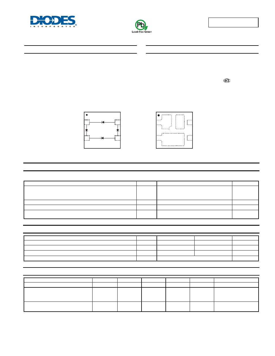
Top View
Device Schematic
Top View
Pin Configuration
2
1
3
4
1
2
4
3
N/C
~
~
-
+