Pds360q, Maximum ratings, Thermal characteristics – Diodes PDS360Q User Manual
Page 2: Electrical characteristics
POWERDI is a registered trademark of Diodes Incorporated.
PDS360Q
Document number: DS36911 Rev. 1 - 2
2 of 5
www.diodes.com
February 2014
© Diodes Incorporated
PDS360Q
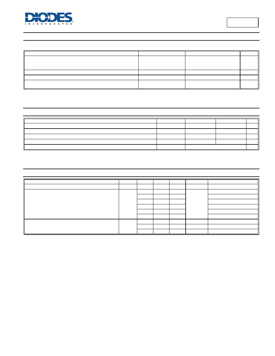
Maximum Ratings
(@T
A
= +25°C, unless otherwise specified.)
Single phase, half wave, 60Hz, resistive or inductive load.
For capacitance load, derate current by 20%.
Characteristic Symbol
Value
Unit
Peak Repetitive Reverse Voltage
Working Peak Reverse Voltage
DC Blocking Voltage
V
RRM
V
RWM
V
R
60 V
RMS Reverse Voltage
V
R(RMS)
42 V
Average Rectified Output Current (See also Figure 4)
I
O
3 A
Non-Repetitive Peak Forward Surge Current
8.3ms Single half sine-wave superimposed on rated load
I
FSM
100 A
Thermal Characteristics
Characteristic Symbol
Typ
Max
Unit
Thermal Resistance Junction to Soldering Point
R
JS
3.0
C/W
Thermal Resistance Junction to Ambient Air (Note 6) T
A
= +25°C
R
JA
95
C/W
Thermal Resistance Junction to Ambient Air (Note 7) T
A
= +25°C
R
JA
70
C/W
Thermal Resistance Junction to Ambient Air (Note 8) T
A
= +25°C
R
JA
50
C/W
Operating and Storage Temperature Range
T
J
, T
STG
-55 to +150
C
Electrical Characteristics
(@T
A
= +25°C, unless otherwise specified.)
Characteristic Symbol
Min
Typ
Max
Unit
Test
Condition
Reverse Breakdown Voltage (Note 8)
V
(BR)R
60
V
I
R
= 0.2mA
Forward Voltage
V
F
0.57 0.62
V
I
F
= 3A, T
J
= +25
C
0.53 0.60
I
F
= 3A, T
J
= +100
C
0.51 0.57
I
F
= 3A, T
J
= +125
C
0.70 0.76
I
F
= 6A, T
J
= +25
C
0.62 0.70
I
F
= 6A, T
J
= +100
C
0.60 0.66
I
F
= 6A, T
J
= +125
C
Reverse Leakage Current (Note 8)
I
R
3 150 μA
T
J
= +25
C, V
R
= 60V
10 mA
T
J
= +100
C, V
R
= 60V
1.5 15 mA
T
J
= +125
C, V
R
= 60V
Notes:
6. FR-4 PCB, 2 oz. Copper, minimum recommended pad layout per http://www.diodes.com.
7. Polymide PCB, 2 oz. Copper, minimum recommended pad layout per http://www.diodes.com.
8. Polymide PCB, 2 oz. Copper. Cathode pad dimensions 9.4 mm x 7.4 mm. Anode pad dimensions 2.7 mm x 1.6 mm.
9. Short duration pulse test used to minimize self-heating effect.