Pds4150, Maximum ratings, Thermal characteristics – Diodes PDS4150 User Manual
Page 2: Electrical characteristics
POWERDI is a registered trademark of Diodes Incorporated.
PDS4150
Document number: DS30473 Rev. 14 - 2
2 of 4
March 2014
© Diodes Incorporated
PDS4150
Maximum Ratings
(@T
A
= +25°C, unless otherwise specified.)
Single phase, half wave, 60Hz, resistive or inductive load.
For capacitance load, derate current by 20%.
Characteristic Symbol
Value
Unit
Peak Repetitive Reverse Voltage
Working Peak Reverse Voltage
DC Blocking Voltage
V
RRM
V
RWM
V
R
150 V
RMS Reverse Voltage
V
R(RMS)
106 V
Average Rectified Output Current (See also Figure 4)
I
O
4 A
Non-Repetitive Peak Forward Surge Current
8.3ms Single half sine-wave Superimposed on Rated Load
I
FSM
180 A
Thermal Characteristics
Characteristic Symbol
Typ
Max
Unit
Thermal Resistance Junction to Soldering Point
R
θJS
⎯
2.0 °C/W
Thermal Resistance Junction to Ambient Air (Note 6) T
A
= +25°C
R
θJA
90
⎯
°C/W
Thermal Resistance Junction to Ambient Air (Note 7) T
A
= +25°C
R
θJA
60
⎯
°C/W
Thermal Resistance Junction to Ambient Air (Note 8) T
A
= +25°C
R
θJA
40
⎯
°C/W
Operating and Storage Temperature Range
T
J
, T
STG
-65 to +175
°C
Electrical Characteristics
(@T
A
= +25°C, unless otherwise specified.)
Characteristic Symbol
Min
Typ
Max
Unit
Test
Condition
Reverse Breakdown Voltage (Note 9)
V
(BR)R
150
⎯
⎯
V
I
R
= 10µA
Forward Voltage
V
F
⎯
⎯
⎯
⎯
0.71
0.57
0.77
0.63
0.76
0.64
0.81
0.70
V
I
F
= 4A, T
S
= +25°C
I
F
= 4A, T
S
= +125°C
I
F
= 8A, T
S
= +25°C
I
F
= 8A, T
S
= +125°C
Reverse Leakage Current (Note 9)
I
R
⎯
⎯
⎯
0.3
0.35
0.4
10
0.8
4.5
µA
mA
mA
T
S
= +25
°C, V
R
= 150V
T
S
= +125
°C, V
R
= 100V
T
S
= +125
°C, V
R
= 150V
Notes:
6. FR-4 PCB, 2 oz. Copper, minimum recommended pad lay
7. Polyimide PCB, 2 oz. Copper, minimum recommended pad layout per
8. Polyimide PCB, 2 oz. Copper. Cathode pad dimensions 9.4mm x 7.2mm. Anode pad dimensions 2.7mm x 1.6mm.
9. Short duration pulse test used to minimize self-heating effect.
0
1
2
3
4
0
1
3
2
4
5
6
7
8
9
10
P
, P
O
WE
R
D
ISSI
P
A
T
IO
N (
W
)
D
I , AVERAGE RECTIFIED OUTPUT CURRENT (A)
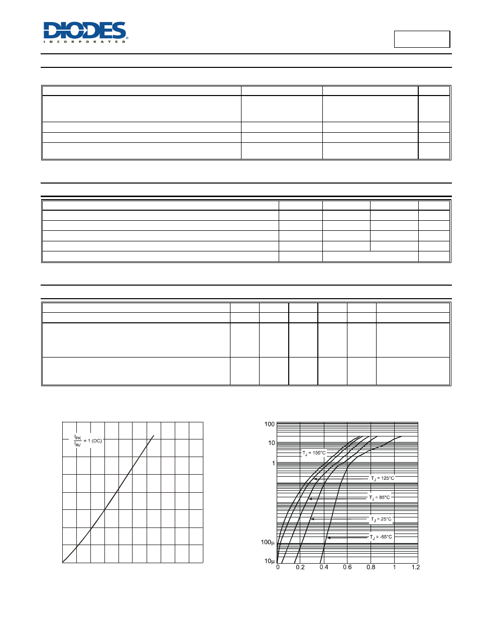
Fig. 1 Forward Power Dissipation
O
V , INSTANTANEOUS FORWARD VOLTAGE (V)
Fig. 2 Typical Forward Characteristics
F
I,
I
N
S
TA
N
TA
N
E
O
U
S F
O
R
WA
R
D
C
U
R
R
E
N
T
(A
)
F
100m
1m
10m