Socket mechanics, Selecting a bga stamped pin socket – Ironwood Electronics SBT User Manual User Manual
Page 3
2 |
P a g e
S B T
. d o c , R e v . C , 6 / 2 8 / 2 0 1 2 , V P
Tel: (800) 404-0204
www.ironwoodelectronics.com
Socket Mechanics
SBT-BGA sockets provide high bandwidth in a small, cost effective ZIF socket for prototype, test and burn-in
applications. SBT-BGA socket is a simple, mechanical socket based on stamped spring pin technology. SBT-
BGA socket is a solder-less socket that can be mounted on to a PCB using supplied hardware. The PCB should
have mounting and alignment holes at proper locations (see page 2 of the drawing for recommended PCB
layout information). Typical SBT-BGA socket footprint is only 5mm larger than the maximum IC size. It is
compatible with the alternate SG-BGA (elastomer) socket footprint. If there are pre-existing holes in the PCB, a
SBT-BGA socket can be custom designed to accommodate those holes (please call Ironwood Tech Support @1-
800-404-0204).
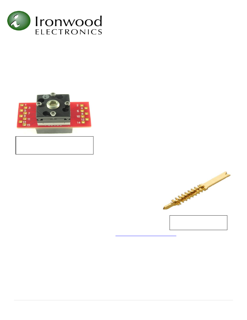
Figure 1 shows a typical stamped spring pin socket. A heat sink
screw on the top provides the compression force as well as thermal
relief and can be customized to dissipate more power. SBT socket
uses SBT contact technology for high endurance and wide
temperature applications. SBT Contact is a stamped contact with
outside spring as well as inside leaf spring that provides a robust
solution for Burn-in & Test applications. The stamped pin used in the
socket is a low-resistance (<0.015
) connector. Figure 2 shows a
picture of the 1mm center – stamped spring pin. SBT contact
technology has 3 part system which includes top plunger, bottom
plunger and a spring. The Beryllium Copper plungers are stamped
and assembled to a stainless steel spring in an automated system to enable fast turnaround time, low cost and
zero defects. The spring probe has high current rating (4.0A continuous for 0.5mm pin and 8A for 1mm pin).
The operating temperature range is -55
to 180
C.
The solder balls from the IC package come in contact with the crown end
of the pin. The bottom end of stamped pin contacts the circuit board pad,
completing an electrical path for the signal. The socket mechanism can be
summarized as a downward force applied on the IC which compresses
solder balls on the spring probe which in turn compresses on the circuit
board and thereby making electrical connection.
Selecting a BGA Stamped pin socket
Please refer to the IC package drawing to select the corresponding BGA
stamped pin socket. Visit the Ironwood website:
Select the “Products” link.
Next, under the “Browse” menu, select the “GHz BGA & MLF Socket (SG, SS, SBT)” link. In the table, select
the part number from the first column which corresponds to your pin count, IC body size, array size, and pitch.
The top webpage frame will show a link to the drawing, a picture of the socket (JPEG format), and provide low-
volume price information. The drawing is a four page PDF file. The first page shows the socket exploded view
and the material details. The second page provides the recommended PCB layout (Note:
BGA pads are not
symmetrical with respect to the mounting holes
). The third page shows the compatible BGA specification.
The fourth page shows more socket views and backing/insulation plate dimensions. Check the BGA pattern and
the following four parameters.
1. IC co-planarity value should be less than or equal to that shown in the table.
2. Maximum total height of IC should be less than or equal to that shown in the table.
Figure 1: Stamped Spring Pin Socket
with Swivel Lid
Figure 2: Picture of 1mm
center - Spring Pin