Daisy-chaining devices, Using an ac reference, Digitally programmable current source – Rainbow Electronics MAX5173 User Manual
Page 13

Daisy-Chaining Devices
The serial data output pin (DOUT) allows multiple
MAX5171/MAX5173s to be daisy-chained together, as
shown in Figure 8. The advantage of this is that only
two lines are needed to control all of the DACs on the
line. The disadvantage is that it takes
n
commands to
program the DACs. Figure 9 shows several MAX5171/
MAX5173s sharing one common DIN signal line. In this
configuration, the data bus is common to all devices.
However, this configuration uses more I/O lines
because each device requires a dedicated CS line.
The benefit is that only one command is needed to pro-
gram any DAC.
Using an AC Reference
The MAX5171/MAX5173 accepts reference voltages
with AC components as long as the reference voltage
remains between 0 and V
DD
- 1.4V. Figure 10 shows a
technique for applying a sine-wave signal to the REF.
The reference voltage must remain above AGND.
Digitally Programmable Current Source
The circuit of Figure 11 places an NPN transistor
(2N3904 or similar) within the op amp feedback loop to
implement a digitally programmable, unidirectional cur-
rent source. The output current is calculated with the
following equation:
where N is the numeric value of the DAC’s binary input
code and R is the sense resistor shown in Figure 11.
I
V
N
R
OUT
REF
=
⋅
⋅
16384
MAX5171/MAX5173
Low-Power, Serial, 14-Bit DACs
with Force/Sense Voltage Output
______________________________________________________________________________________
13
DAC CONTENTS
MSB
LSB
11 1111 1111 1111
10 0000 0000 0001
2
·
V
REF
(8193/16384)
2
·
V
REF
(16383/16384)
ANALOG OUTPUT
10 0000 0000 0000
2
·
V
REF
(8192/16384)
01 1111 1111 1111
2
·
V
REF
(8191/16384)
00 0000 0000 0001
2
·
V
REF
(1/16384)
00 0000 0000 0000
0
DAC
V
OUT
V+
V-
+5V/+3.3V
REF
10k
10k
FB
OUT
V
DD
GND
MAX5171
MAX5173
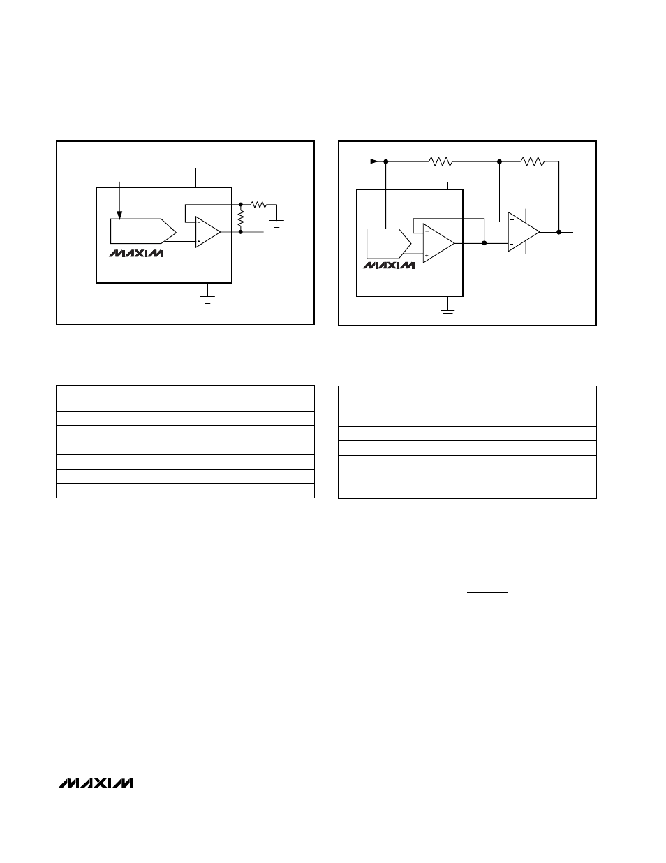
Figure 7. Bipolar Output Circuit
Table 2. Unipolar Code Table
(Circuit of Figure 6)
Table 3. Bipolar Code Table
(Circuit of Figure 7)
MAX5171
MAX5173
DAC
REF
OUT
10k
10k
GND
+5V/+3.3V
V
DD
FB
Figure 6. Unipolar Output Circuit (Rail-to-Rail)
DAC CONTENTS
MSB
LSB
11 1111 1111 1111
10 0000 0000 0001
+V
REF
[(2
·
8193/16384) - 1]
+V
REF
[(2
·
16383/16384) - 1]
ANALOG OUTPUT
01 1111 1111 1111
+V
REF
[(2
·
8191/16384) - 1]
00 0000 0000 0001
+V
REF
[(2
·
1/16384) - 1]
10 0000 0000 0000
+V
REF
[(2
·
8192/16384) - 1]
00 0000 0000 0000
-V
REF
