Detailed description – Rainbow Electronics MAX5173 User Manual
Page 10

MAX5171/MAX5173
Low-Power, Serial, 14-Bit DACs
with Force/Sense Voltage Output
10
______________________________________________________________________________________
Detailed Description
The MAX5171/MAX5173 14-bit, serial, voltage-output
DACs operate with a 3-wire serial interface. These
devices include a 16-bit shift register and a double-
buffered input composed of an input register and a
DAC register (see
Functional Diagram
). In addition, the
negative terminal of the output amplifier is available.
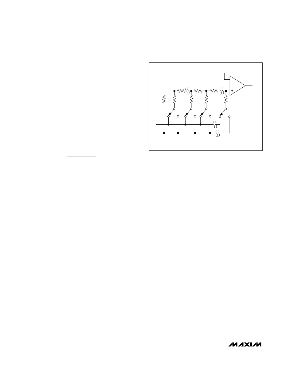
The DACs are designed with an inverted R-2R ladder
network (Figure 1), which produces a weighted voltage
proportional to the reference voltage.
Reference Input
The reference input accepts both AC and DC values
with a voltage range extending from 0 to V
DD
- 1.4V.
The following equation represents the resulting output
voltage:
where N is the numeric value of the DAC’s binary input
code (0 to 16383), V
REF
is the reference voltage, and
Gain is the externally set voltage gain. The maximum
output voltage is V
DD
. The reference pin has a mini-
mum impedance of 18k
Ω
and is code dependent.
Output Amplifier
The MAX5171/MAX5173’s DAC output is internally
buffered by a precision amplifier with a typical slew rate
of 0.6V/µs. Access to the output amplifier’s inverting
input provides flexibility in output gain setting and sig-
nal conditioning (see
Applications Information
).
The output amplifier settles to ±0.5LSB from a full-scale
transition within 12µs, when loaded with 5k
Ω
in parallel
with 100pF. Loads less than 2k
Ω
degrade performance.
Shutdown Mode
The MAX5171/MAX5173 feature a software- and hard-
ware-programmable shutdown mode that reduces the
typical supply current to 1µA. Enter shutdown by writing
the appropriate input-control word as shown in Table 1,
or by using the hardware shutdown. In shutdown mode,
the reference input and amplifier output become high-
impedance, and the serial interface remains active.
Data in the input register is saved, allowing the
MAX5171/MAX5173 to recall the prior output state
when returning to normal operation. To exit shutdown,
reload the DAC register from the shift register by simul-
taneously loading the input and DAC registers or by
toggling PDL. When returning from shutdown, wait 40µs
for the output to settle.
Power-Down Lockout
Power-down lockout disables the software/hardware
shutdown mode. A high-to-low transition on PDL brings
the device out of shutdown, returning the output to its
previous state.
Shutdown
Pulling SHDN high while PDL is high places the
MAX5171/MAX5173 in shutdown mode. Pulling SHDN
low does not return the device to normal operation. A
high-to-low transition on PDL or an appropriate com-
mand from the serial data line is required to exit shut-
down (see Table 1 for commands).
Serial Interface
The MAX5171/MAX5173 3-wire serial interface is com-
patible with SPI/QSPI (Figure 2) and MICROWIRE
(Figure 3) interface standards. The 16-bit serial input
word consists of two control bits and 14 bits of data
(MSB to LSB).
The control bits determine the MAX5171/MAX5173’s
response as outlined in Table 1. The MAX5171/
MAX5173’s digital inputs are double buffered, which
allows any of the following:
• Loading the input register without updating the DAC
register.
• Updating the DAC register from the input register.
• Updating the input and DAC registers simultaneously.
V
V
N Gain
OUT
REF
=
⋅ ⋅
16384
OUT
FB
SHOWN FOR ALL 1s ON DAC
D11
2R
2R
2R
2R
2R
R
R
R
REF
AGND
Figure 1. Simplified DAC Circuit Diagram
