Br9016 af-w / arfv-w / arfvm-w – Rainbow Electronics br9080af-w User Manual
Page 8
BR9080AF-W / BR9080ARFV-W / BR9080ARFVM-W /
Memory ICs
BR9016AF-W / BR9016ARFV-W / BR9016ARFVM-W
8/12
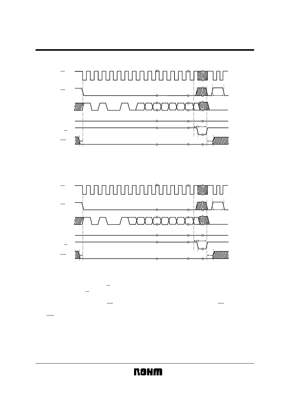
(4) Write cycle
BR9080AF-W / ARFV-W / ARFVM-W
Fig.6 BR9080AF-W / ARFV-W / ARFVM-W
1
4
8
16
32
1
HIGH-Z
HIGH-Z
H
SK
CS
DI
DO
R / B
WC
L
H
L
H
L
H
0
1
0
0
1
0
A0
A1
A7
A8
D0
D15
t
WCH
t
WCS
t
SV
t
E-W
t
CS
BR9016 AF-W / ARFV-W / ARFVM-W
Fig.7 BR9016AF-W / ARFV-W / ARFVM-W
1
4
8
16
32
1
HIGH-Z
HIGH-Z
H
SK
CS
DI
DO
R / B
WC
L
H
L
H
L
H
0
1
0
0
1
A0
A1
A2
A8
A9
D0
D15
t
WCH
t
WCS
t
SV
t
E-W
t
CS
1) At the rising edge of 32nd clock, R / B pin will be come out “LOW” after the specified time delay (tSV).
2) From above edge R / B will indicate the ready / busy status of the chip: “LOW” indicated programming is all in
progress: “HIGH” indicates the write cycle is complete and this part is ready for another instruction.
3) During the input of Write command, CS must be “LOW”. However, once the write operation started, CS could be either
“HIGH” or “LOW”.
4) If WC becomes “HIGH” during Write Cycle, the write operation is halted. In this case, the address data in writing is no
guaranteed. It is necessary to rewrite it.