Rainbow Electronics br9080af-w User Manual
Page 6
BR9080AF-W / BR9080ARFV-W / BR9080ARFVM-W /
Memory ICs
BR9016AF-W / BR9016ARFV-W / BR9016ARFVM-W
6/12
!
!
!
!
Circuit operation
(1) Command mode
BR9080A
1010
100 A0
A1 A2 A3 A4 A5 A6 A7 A8
A1 A2 A3 A4 A5 A6 A7 A8
1010
010 A0
1010
0011
∗ ∗ ∗ ∗ ∗ ∗ ∗ ∗
∗ ∗ ∗ ∗ ∗ ∗ ∗ ∗
D0 D1
−
D14 D15
1010
0000
Read (READ)
Write (WRITE)
Write enable (WEN)
Write disable (WDS)
∗
: Means either V
IH
or V
IL
Address and data are transferred from LSB.
Instruction
Start Bit
Op Code
Address
Data
BR9016A
1010
10 A0 A1
A2 A3 A4 A5 A6 A7 A8 A9
A2 A3 A4 A5 A6 A7 A8 A9
1010
01 A0 A1
1010
0011
∗ ∗ ∗ ∗ ∗ ∗ ∗ ∗
∗ ∗ ∗ ∗ ∗ ∗ ∗ ∗
D0 D1
−
D14 D15
1010
0000
Read (READ)
Write (WRITE)
Write enable (WEN)
Write disable (WDS)
∗
: Means either V
IH
or V
IL
Address and data are transferred from LSB.
Instruction
Start Bit
Op Code
Address
Data
(2) Writing enabled / disabled
High or LOW
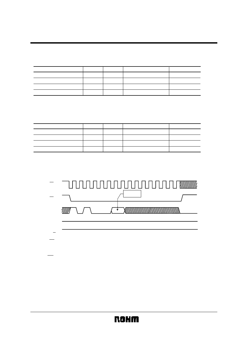
Fig.3
1
1
HIGH-Z
H
SK
CS
DI
DO
R / B
WC
L
H
L
H
L
H
0
1
0
0
0
4
8
ENABLE
=
11
DISABLE
=
00
12
16
1) When CS is “HIGH” during power up, BR9080AF-W / ARFV-W / ARFVM-W, BR9016AF-W / ARFV-W / ARFVM-W
comes up in the write disabled (WDS) state. In order to be programmable, it must receive a write enable (WEN)
instruction.
The device remains programmable until a disable (WDS) instruction is entered, or until it is powered down.
2) It is unnecessary to add the clock after 16th clock.