Br9016 af-w / arfv-w / arfvm-w, And t, Timing, the t – Rainbow Electronics br9080af-w User Manual
Page 7
BR9080AF-W / BR9080ARFV-W / BR9080ARFVM-W /
Memory ICs
BR9016AF-W / BR9016ARFV-W / BR9016ARFVM-W
7/12
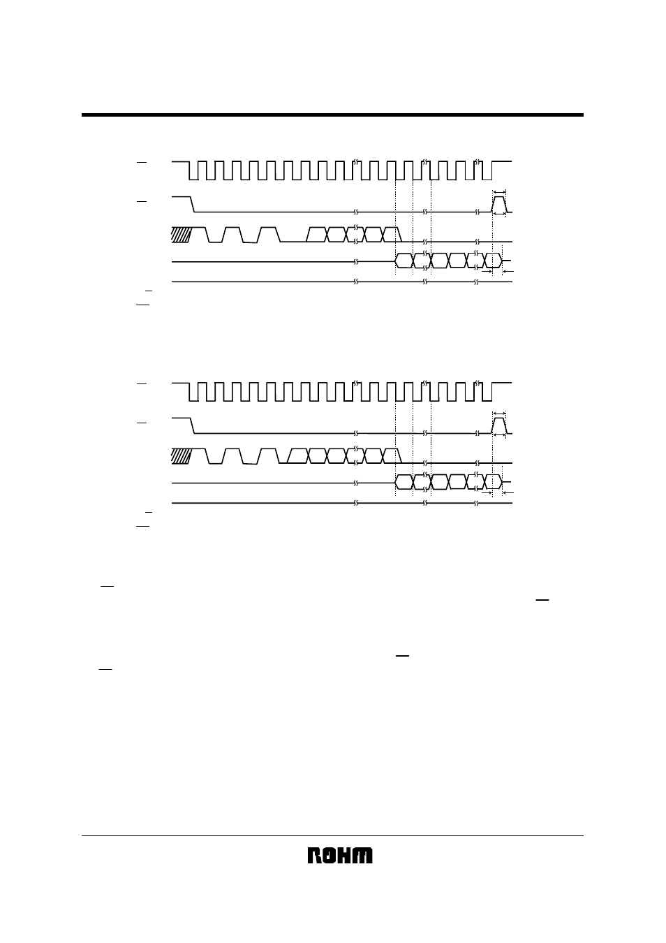
(3) Read cycle
BR9080AF-W / ARFV-W / ARFVM-W
High or LOW
Fig.4 BR9080AF-W / ARFV-W / ARFVM-W
1
4
8
16
32
48
1
HIGH-Z
H
SK
CS
DI
DO
R / B
WC
L
H
L
H
L
H
0
1
1
0
0
0
A0
A1
A7
A8
D0
Read Data (n)
Read Data (n+1)
D15
D15
D0
HIGH-Z
STANDBY
t
CS
t
OH
BR9016 AF-W / ARFV-W / ARFVM-W
High or LOW
Fig.5 BR9016AF-W / ARFV-W / ARFVM-W
1
4
8
16
32
48
1
HIGH-Z
H
SK
CS
DI
DO
R / B
WC
L
H
L
H
L
H
0
1
1
0
0
A1
A2
A0
A8
A9
D0
Read Data (n)
Read Data (n+1)
D15
D15
D0
HIGH-Z
STANDBY
t
CS
t
OH
1) After the fall of the 16th clock pulse, 16-bit data is output from the DO pin in synchronization with the falling edge of the
SK signal.
(DO output changes at a time lag of t
PD0
, t
PD1
because of internal circuit delay following the falling edge of the SK signal.
During the t
PD0
and t
PD1
timing, the t
PD
time should be assured before data is read, to avoid the previous data being lost.
See the synchronized data input / output timing chart in Fig.2.)
2) The data stored in the next address is clocked out of the device on the falling edge of 32nd clock. The data stored in
the upper address every 16 clocks is output sequentially by the continual SK input. Also the read operation is reset by
CS High.