Rainbow Electronics br9080af-w User Manual
Page 5
BR9080AF-W / BR9080ARFV-W / BR9080ARFVM-W /
Memory ICs
BR9016AF-W / BR9016ARFV-W / BR9016ARFVM-W
5/12
!
!
!
!
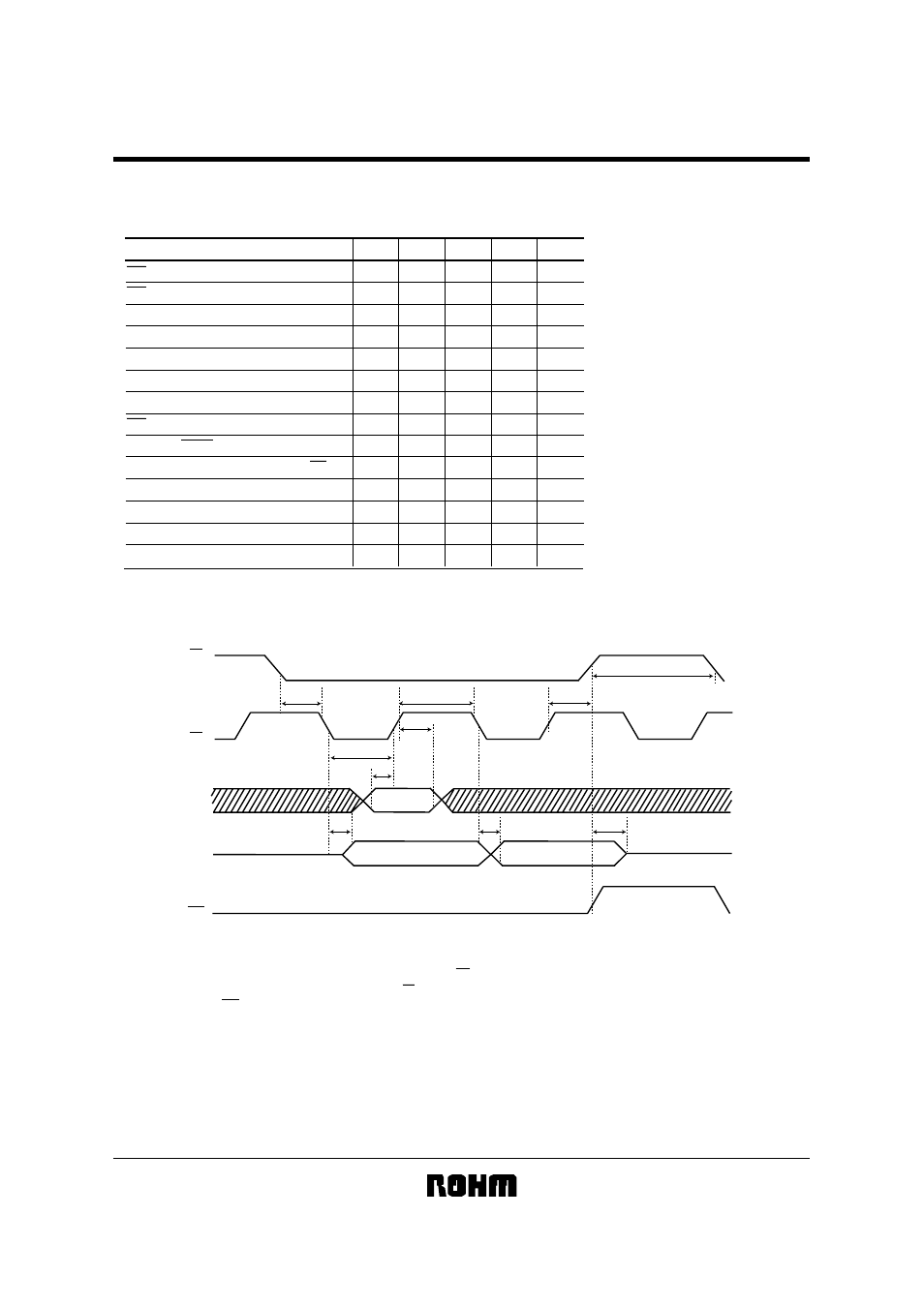
Operating timing characteristics
BR9080AF-W / ARFV-W / ARFVM-W, BR9016AF-W / ARFV-W / ARFVM-W
(Unless otherwise noted, Ta=
−40∼85°C, V
CC
=2.7V
∼5.5V)
Parameter
Symbol
Min.
Typ.
Max.
Unit
f
CSS
100
−
−
ns
t
CSH
100
−
−
ns
t
WCH
100
−
−
ns
t
DIS
100
−
−
ns
t
DIH
−
−
150
ns
t
PD1
−
−
150
ns
t
PD0
−
−
10
ms
t
E / W
250
−
−
ns
t
CS
−
−
150
ns
t
SV
0
−
150
ns
t
OH
230
−
−
ns
t
WH
230
−
−
ns
t
WL
0
−
−
ns
0
−
−
ns
t
WCS
CS setup time
Time when DO goes HIGH-Z (via CS)
Data clock high level time
Write control hold time
Data setup time
Data hold time
DO rise delay time
DO fall delay time
Self-timing programming cycle
CS minimum high level time
READY / BUSY display valid time
CS hold time
Data clock low level time
Write control setup time
!
!
!
!
Timing chart
Synchronous Data Input Output Timing
CS
SK
DI
DO
WC
t
DIS
t
DIH
t
CSS
t
PD
t
OH
t
CSH
t
CS
t
PD
t
WL
t
WH
· Input data are clocked in to DI at the rising edge of the clock (SK).
· Output data will toggle on the falling edge of the SK clock.
· The WC pin does not have any effect on the READ, EWEN and EWDS operations.
Fig.2