Detailed description, Table 1. on/off logic control, On/off control – Rainbow Electronics MAX849 User Manual
Page 9: Operating modes
MAX848/MAX849
1-Cell to 3-Cell, High-Power,
Low-Noise, Step-Up DC-DC Converters
_______________________________________________________________________________________
9
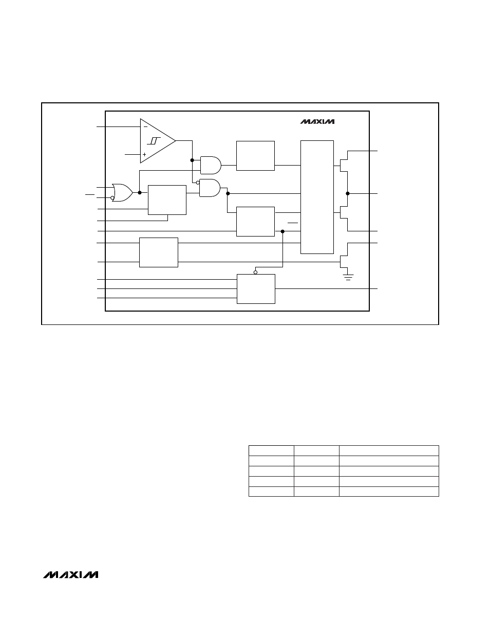
_______________Detailed Description
The MAX848/MAX849 combine a switching regulator,
N-channel power MOSFET, P-channel synchronous
rectifier, precision reference voltage, power-good indi-
cator, and battery voltage monitor, all in a single mono-
lithic device. The MAX848/MAX849 are powered
directly from the output. The output voltage is factory
preset to 3.3V or adjustable from 2.7V to 5V with exter-
nal resistors (Dual Mode™ operation). These devices
start from a low 1V input voltage and remain opera-
tional down to 0.7V. The MAX848/MAX849 operate with
either one to three NiCd/NiMH cells or one Li-Ion cell.
At power-up, an internal low-voltage oscillator drives
the N-channel power switch, and the output voltage
slowly builds up. The oscillator has a 25% nominal duty
cycle to prevent current build-up in the inductor. An
output voltage in excess of the nominal 2.25V lockout
voltage activates the error comparator and internal tim-
ing circuitry. The device resumes operation in either
pulse-frequency-modulation (PFM) low-power mode or
pulse-width-modulation (PWM) low-noise mode, select-
ed by the logic control, CLK/SEL. Figure 2 shows the
standard application circuit for the MAX849 configured
in the high-power PWM mode.
On/Off Control
The MAX848/MAX849 are turned on or off by logic
input pins ON1 and ON2 (Table 1). When ON1 = 1 or
ON2 = 0, the part is on. When ON1 = 0 and ON2 = 1,
the part is off. Both inputs have logic trip points near
0.5 x V
OUT
with 0.15 x V
OUT
hysteresis.
Operating Modes
The MAX848/MAX849 operate in either PFM, PWM, or
PWM synchronized to an externally applied clock sig-
nal. Table 2 lists each operating mode.
ON
REF
1.25V
RDY
EN
START-UP
OSCILLATOR
Q
OUT
ON1
ON2
REF
GND
CLK/SEL
FB
POKIN
AINSEL
AIN1
AIN2
EN
ADC
FEEDBACK
EN
300kHz
OSCILLATOR
2.25V
FEEDBACK
AND
POWER-GOOD
SELECT
PFM/PWM
PCH
0.25
Ω
NCH
0.13
Ω
POUT
LX
PGND
POK
DATA
MAX848/MAX849
N
Q
Q
D
EN
OSC
MODE
PFM/PWM
CONTROLLER
Figure 1. Functional Diagram
ON1
O
ON
N2
2
MAX848/MAX849
0
0
On
0
1
Off
1
0
On
1
1
On
Table 1. On/Off Logic Control