Table 2. selecting operating mode, Setting the output voltage externally – Rainbow Electronics MAX849 User Manual
Page 10
MAX848/MAX849
1-Cell to 3-Cell, High-Power,
Low-Noise, Step-Up DC-DC Converters
10
______________________________________________________________________________________
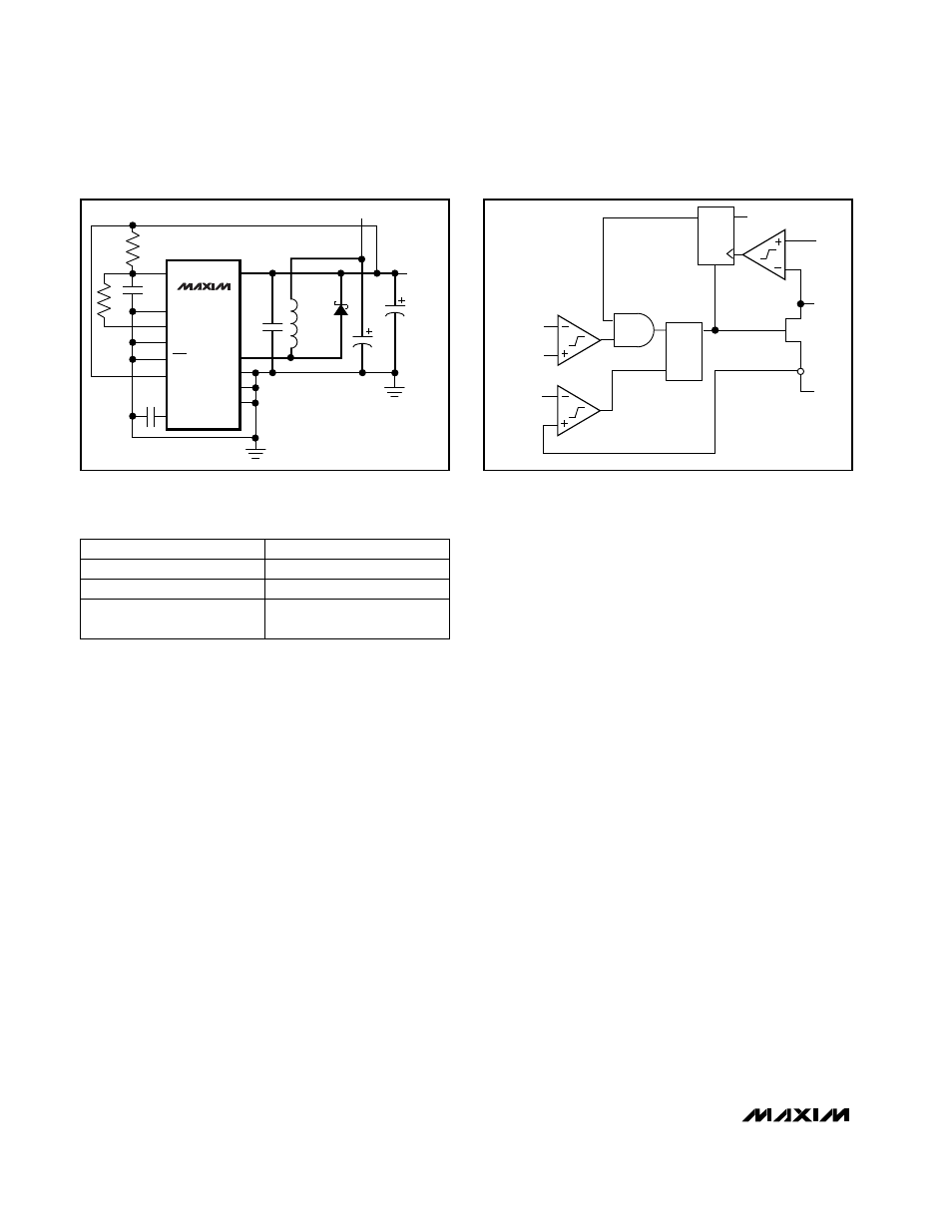
Low-Power PFM Mode
When CLK/SEL is pulled low, the MAX848/MAX849 oper-
ate in low-power, low-supply-current PFM mode. Pulse-
frequency modulation provides the highest efficiency at
light loads. The P-channel rectifier is turned off to reduce
gate-charge losses, and the regulator operates in dis-
continuous mode. The N-channel power MOSFET is kept
on until the inductor current ramps to 30% of the current
limit. The inductor energy is delivered to the output
capacitor when the switch turns off. A new cycle is inhib-
ited until the inductor current crosses zero. Zero current
detection is accomplished by sensing the LX voltage
crossing the output voltage. Figure 3 shows the block
diagram for the PFM controller.
Low-Noise PWM Mode
When CLK/SEL is pulled high, the MAX848/MAX849
operate in high-power, low-noise, current-mode PWM,
switching at the 300kHz nominal internal oscillator fre-
quency. The internal rectifier is active in this mode,
and the regulator operates in continuous mode. The
N-channel power MOSFET turns on until either the output
voltage is in regulation or the inductor current limit is
reached (0.8A for the MAX848 and 1.4A for the
MAX849). The switch turns off for the remainder of the
cycle and the inductor energy is delivered to the output
capacitor. A new cycle is initiated on the next oscillator
cycle. In low-noise applications, the fundamental and the
harmonics generated by the fixed switching frequency
can easily be filtered. Figure 4 shows the block diagram
for the PWM controller.
The MAX848/MAX849 enter synchronized current-mode
PWM when a clock signal (200kHz < f
CLK
< 400kHz) is
applied to CLK/SEL. The internal synchronous rectifier
is active and the switching frequency is synchronized
to the externally applied clock signal. For wireless
applications, this ensures that the harmonics of the
switching frequencies are predictable and can be kept
outside the IF band(s). High-frequency operation per-
mits low-magnitude output ripple voltage.
The MAX848/MAX849 are capable of providing a stable
output even with a rapidly pulsing load (GSM, DECT),
such as from a transmitter power amplifier in digital cord-
less phones (see
Typical Operating Characteristics
).
In PWM mode, the use of the synchronous rectifier
ensures constant-frequency operation, regardless of
the load current.
Setting the Output Voltage Externally
The MAX848/MAX849 feature Dual Mode operation.
The output voltage is preset to 3.3V (FB = 0V), or it can
be adjusted from 2.7V to 5.5V with external resistors
R1, R2, and R3, as shown in Figure 5. To set the output
voltage externally, select resistor R3 in the 10k
Ω
to
100k
Ω
range. The values for R1 and R2 are given by:
R2 = R3(V
OUT
/ V
TRIP
- 1)
R1 = (R3 + R2)(V
TRIP
/ V
REF
- 1)
MAX849
C5
0.1
µ
F
V
IN
= 1.1V
C2
0.1
µ
F
C3
0.22
µ
F
C1
22
µ
F
OUT
GND
POK
ON1
ON2
CLK/SEL
REF
PGND
FB
POKIN
LX
POUT
C4
2 x 100
µ
F
L1
10
µ
H
D1
MBR0520L
3.3V @
200mA
R3
100k
10
Ω
*
HEAVY LINES INDICATE
HIGH-CURRENT PATH.
*
Figure 2. 3.3V Preset Output
Table 2. Selecting Operating Mode
CLK/SEL
MODE
0
PFM
1
PWM
External clock
(200kHz ~ 400kHz)
Synchronized PWM
R
S
Q
R
D
Q
PFM-MODE
CURRENT-
LIMIT LEVEL
REF
FEEDBACK
POUT
LX
PGND
LOGIC HIGH
N
CURRENT
SENSE
Figure 3. Controller Block Diagram in PFM Mode