Pin description – Rainbow Electronics MAX849 User Manual
Page 8
MAX848/MAX849
1-Cell to 3-Cell, High-Power,
Low-Noise, Step-Up DC-DC Converters
8
_______________________________________________________________________________________
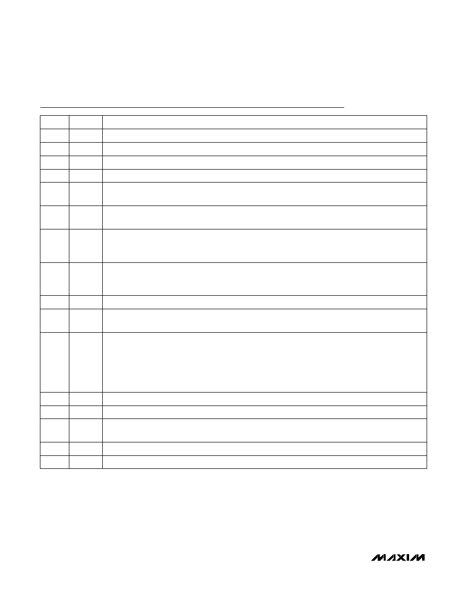
Pin Description
ADC’s Input Channel Selector. Pull low to select AIN1 and drive high to select AIN2.
AINSEL
9
ADC’s Serial Output. Pulsed output, RZ format. Full scale is f
OSC
/2 (f
CLK
/2 in external sync mode). The
DATA output is low when V
CLK/SEL
= 0V (PFM mode).
DATA
10
External Clock Input/Regulator’s Switching Mode Selector.
CLK/SEL = low: low-power, low-quiescent PFM mode. Delivers 100mW of output power.
CLK/SEL = high: low-noise, high-power PWM mode, switching at a constant frequency (300kHz).
CLK/SEL = driven with external clock: low-noise, high-power, synchronized PWM mode. The internal
oscillator is synchronized to the external clock (200kHz ~ 400kHz). Turning the DC-DC converter on with
V
CLK/SEL
= 0V also serves as a soft-start function, since the peak inductor current is limited to 30% of the
nominal value.
CLK/SEL
11
Source of the Internal N-Channel Power MOSFET. Connect to high-current ground path.
PGND
12
Drain of the Internal N-Channel Power MOSFET and P-Channel Synchronous Rectifier
LX
13
Output Sense Input. The IC is powered from OUT. Bypass to GND with a 0.1µF ceramic capacitor. Connect
OUT to POUT through a 10
Ω
series resistor.
OUT
5
Power-Good Comparator Input. Connect to GND for fixed threshold (V
OUT
x 0.9). To adjust the threshold,
connect to a resistor divider from OUT to GND.
POKIN
6
Dual Mode DC-DC Converter Feedback Input. Connect to GND for fixed 3.3V output voltage. Connect to
a resistor divider from OUT to GND to adjust the output voltage. Minimize noise coupling from switching
signals to FB.
FB
7
Power-Good Output. This open-drain output is pulled low when the output voltage (V
OUT
) drops below
the internally set threshold (fixed threshold), or when the voltage at POKIN drops below V
REF
(adjustable
threshold).
POK
8
Ground. Use for low-current ground paths. Connect to PGND with a short trace.
GND
4
Reference Output. Bypass with a 0.22µF capacitor to GND.
REF
3
PIN
ADC’s Channel 2 Input. Analog input voltage range is 0V to 2.5V.
AIN2
2
ADC’s Channel 1 Input. Analog input voltage range is 0.625V to 1.875V.
AIN1
1
FUNCTION
NAME
14
POUT
Source of the Internal P-Channel Synchronous Rectifier MOSFET. Connect an external Schottky diode from
LX to POUT. Bypass to PGND with a 0.1µF ceramic capacitor as close to the IC as possible.
15
ON2
OFF Control Input. When ON1 = 0 and ON2 = 1, the IC is off.
16
ON1
ON Control Input. When ON1 = 1 or ON2 = 0, the IC is on.