Rainbow Electronics MAX849 User Manual
Page 11
MAX848/MAX849
1-Cell to 3-Cell, High-Power,
Low-Noise, Step-Up DC-DC Converters
______________________________________________________________________________________
11
where V
REF
= 1.25V, V
OUT
is the desired output volt-
age, and V
TRIP
is the desired trip level for the power-
good comparator.
Power-OK
The MAX848/MAX849 feature a power-good compara-
tor. This comparator’s open-drain output, POK, is
pulled low when the output voltage falls below the nom-
inal internal threshold level of 3V with POKIN = 0V. To
set the power-good trip level externally, refer to the
Setting the Output Voltage Externally
section.
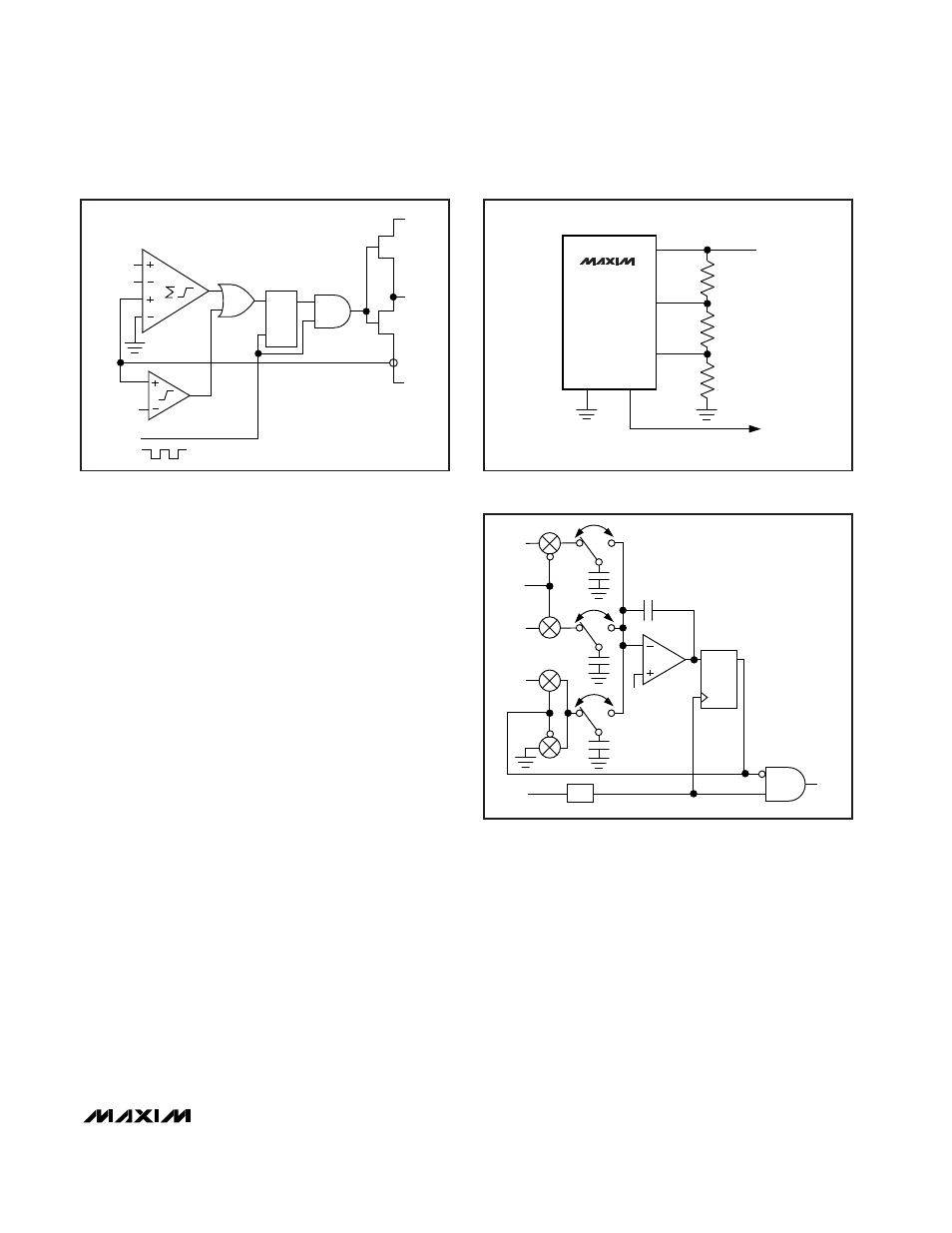
Analog-to-Digital Converter (ADC)
The MAX848/MAX849 have an internal, two-channel, seri-
al ADC. The ADC converts an analog input voltage into a
digital stream available at the DATA pin. The converter
skips clock pulses in proportion to the input voltage.
Output format is a return-to-zero bit stream with a bit
duration of 1/f
CLK
. At zero-scale input voltage, all pulses
are skipped and DATA remains low; with a positive full-
scale input voltage, no pulses are skipped; and at mid-
scale, every other pulse is skipped. The ADC’s clock is
one-half of the externally applied clock signal or one-half
of the internal 300kHz clock available at LX. In PFM
mode, the converter is not active and DATA is driven low.
Channel 1, AIN1, has an input voltage range of 0.625V
to 1.875V and is selected when AINSEL is low. Channel
2, AIN2, accepts inputs in the 0V to 2.5V range and is
selected when AINSEL is pulled high (Figure 6).
The ADC is a switched-capacitor type; therefore, an
anti-aliasing filter might be required at the inputs. Insert
a 1k
Ω
series resistor and a 0.01µF filter capacitor in
noisy environments.
Timer Function Implementation
Implement the necessary counter functions either with
discrete hardware or with microcontroller (µC) imple-
mentations. The output resolution depends on how
many of the ADC clock pulses are counted, as shown
in Figure 7.
Hardware Implementation
A complete hardware solution can be implemented
using either two counters or an ASIC. Resolution
depends on how many pulses are counted. The main
advantage of the discrete hardware implementation is
that accuracy is not affected by interrupt latency asso-
ciated with the µC solution.
R
S
Q
OSC
PWM-MODE
CURRENT-
LIMIT LEVEL
REF
FEEDBACK
POUT
LX
PGND
N
P
Figure 4. Controller Block Diagram in PWM Mode
MAX848
MAX849
OUT
POKIN
FB
POK
GND
OUTPUT
R1
R2
R3
Figure 5. Adjustable Output Voltage and Power-Good Trip Level
C/2
C/2
C
REF
C
D
Q
÷
2
2 x REF
AIN2
OSC
AINSEL
AIN1
DATA
Figure 6. A/D Converter Block Diagram