Electrical characteristics – Rainbow Electronics MAX849 User Manual
Page 4
MAX848/MAX849
1-Cell to 3-Cell, High-Power,
Low-Noise, Step-Up DC-DC Converters
4
_______________________________________________________________________________________
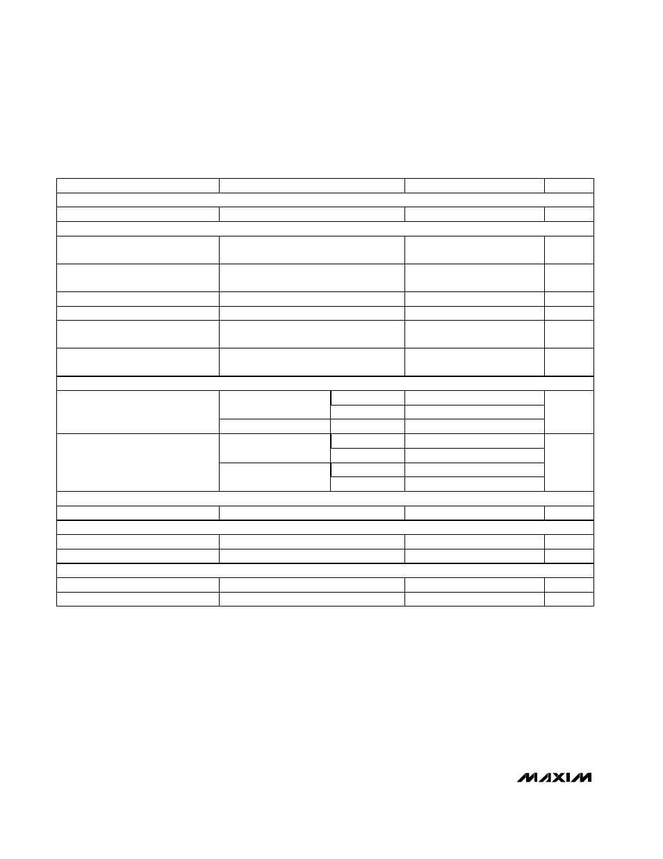
ELECTRICAL CHARACTERISTICS
(V
OUT
= 3.6V, GND = PGND = CLK/SEL = ON1 = ON2 = AINSEL = AIN1 = AIN2 = FB = POKIN, POUT = OUT,
T
A
= -40°C to +85°C
,
unless otherwise noted.) (Note 9)
Note 1:
Minimum operating voltage. Because the MAX848/MAX849 are bootstrapped to the output, it will operate down to a 0.7V input.
Note 2:
In low-power mode (CLK/SEL = GND), the output voltage regulates 1% higher than in low-noise mode (CLK/SEL = OUT or
synchronized).
Note 3:
The part is in start-up mode until it reaches this voltage level. Do not apply full-load current.
Note 4:
Load regulation is measured from no load to full load, where full load is determined by the N-channel switch current limit.
Note 5:
Start-up is tested with Figure 2’s circuit. Output current is measured when the input and output voltages are applied.
Note 6:
Supply current from the 3.34V output is measured between the 3.34V output and the OUT pin. This current correlates directly
with actual battery supply current, but is reduced in value according to the step-up ratio and efficiency. V
OUT
= 3.6V to keep
the internal switch open when measuring the current into the device.
Note 7:
When V
CLK/SEL
= 0V, the inductor is forced into constant-peak-current, discontinuous operation. This is guaranteed by
testing in Figure 2’s circuit.
Note 8:
ON1 and ON2 inputs have approximately 0.15V
OUT
hysteresis.
Note 9:
Specifications to -40°C are guaranteed by design, not production tested.
%
80
90
Oscillator Maximum Duty Cycle
kHz
260
340
CLK/SEL = OUT
Internal Oscillator Frequency
V
1.225
1.275
Rising V
POKIN
External Trip Level
V
2.95
3.10
Rising V
OUT
, V
POKIN
< 0.1V
Internal Trip Level
% FSR
±4
f
CLK
= 400kHz, 5ms conversion
Accuracy
250
550
MAX849
CLK/SEL = GND (Note 7)
N-Channel Current Limit
120
300
MAX848
PARAMETER
CONDITIONS
MIN
TYP
MAX
UNITS
1100
1800
MAX849
CLK/SEL = OUT
mA
600
1100
MAX848
0.5
CLK/SEL = OUT
P-channel
Switch On-Resistance
0.25
CLK/SEL = OUT
N-channel
I
REF
= 0mA
Reference Output Voltage
1.225
1.275
V
Ω
Output Voltage (Note 3)
V
FB
< 0.1V, CLK/SEL = OUT,
includes load-regulation error
3.13
3.47
V
FB Regulation Voltage
Adjustable output, CLK/SEL = OUT
1.21
1.27
V
Output Voltage Lockout Range
(Note 3)
2.05
2.45
V
0.6
CLK/SEL = GND
µA
300
CLK/SEL = OUT, does not include
switching losses
OUT Supply Current in Low-Noise
Mode (Note 6)
µA
90
CLK/SEL = GND
OUT Supply Current in Low-Power
Mode (Note 6)
OUT Supply Current in Shutdown
V
ON2
= 3.6V
20
µA
REFERENCE
DC-DC CONVERTER
DC-DC SWITCHES
ADC
POWER-GOOD
LOGIC CONTROL INPUTS