Applications information – Rainbow Electronics MAX1448 User Manual
Page 12
MAX1448
10-Bit, 80Msps, Single +3.0V, Low-Power
ADC with Internal Reference
12
______________________________________________________________________________________
data is valid on the rising edge of the input clock. The
output data has an internal latency of 5.5 clock cycles.
Figure 6 also shows the relationship between the input
clock parameters and the valid output data.
Applications Information
Figure 7 shows a typical application circuit containing a
single-ended to differential converter. The internal refer-
ence provides a V
DD
/2 output voltage for level shifting
purposes. The input is buffered and then split to a volt-
age follower and inverter. A lowpass filter follows the op
amps to suppress some of the wideband noise associ-
ated with high-speed op amps. The user may select the
R
ISO
and C
IN
values to optimize the filter performance
to suit a particular application. For the application in
Figure 7, an RISO of 50
Ω is placed before the capaci-
tive load to prevent ringing and oscillation. The 22pF
C
IN
capacitor acts as a small bypassing capacitor.
50
60
80
70
90
100
20
40
30
50
60
70
CLOCK DUTY CYCLE (%)
SFDR (dBc)
f
IN
= 25.12MHz AT -0.5dB FS
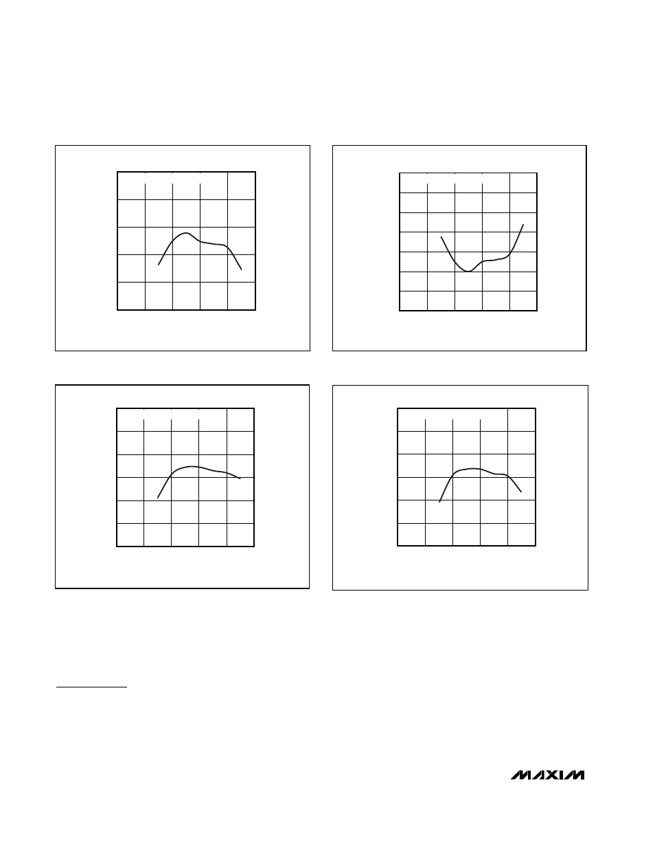
Figure 3a. Spurious Free Dynamic Range vs. Clock Duty
Cycle (Differential Input)
52
56
54
60
58
62
64
20
40
30
50
60
70
CLOCK DUTY CYCLE (%)
SNR (dB)
f
IN
= 25.12MHz AT -0.5dB FS
Figure 3b. Signal-to-Noise Ratio vs. Clock Duty Cycle
(Differential Input)
-85
-75
-80
-65
-70
-55
-60
-50
20
40
30
50
60
70
CLOCK DUTY CYCLE (%)
THD (dBc)
f
IN
= 25.12MHz AT -0.5dB FS
Figure 4a. Total Harmonic Distortion vs. Clock Duty Cycle
(Differential Input)
52
56
54
60
58
62
64
20
40
30
50
60
70
CLOCK DUTY CYCLE (%)
SINAD (dB)
f
IN
= 25.12MHz AT -0.5dB FS
Figure 4b. Signal-to-Noise Plus Distortion vs. Clock Duty Cycle
(Differential Input)