Detailed description – Rainbow Electronics MAX1448 User Manual
Page 10
MAX1448
10-Bit, 80Msps, Single +3.0V, Low-Power
ADC with Internal Reference
10
______________________________________________________________________________________
_______________Detailed Description
The MAX1448 uses a 10-stage, fully differential,
pipelined architecture (Figure 1) that allows for high-
speed conversion while minimizing power consump-
tion. Each sample moves through a pipeline stage
every half clock-cycle. Counting the delay through the
output latch, the clock-cycle latency is 5.5.
A 1.5-bit (2-comparator) flash ADC converts the held
input voltage into a digital code. The following digital-
to-analog converter (DAC) converts the digitized result
back into an analog voltage, which is then subtracted
from the original held input signal. The resulting error
signal is then multiplied by two, and the product is
passed along to the next pipeline stage where the
process is repeated. Each stage provides a 1-bit reso-
lution. Digital error correction compensates for ADC
comparator offsets in each pipeline stage and ensures
no missing codes.
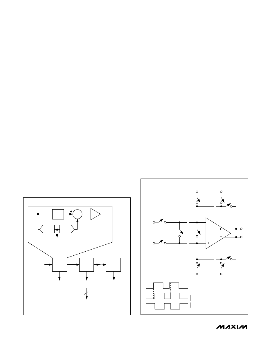
Input Track-and-Hold Circuit
Figure 2 displays a simplified functional diagram of the
input track-and-hold (T/H) circuit in both track and hold
mode. In track mode, switches S1, S2a, S2b, S4a, S4b,
S5a, and S5b are closed. The fully differential circuit
samples the input signal onto the two capacitors (C2a
and C2b) through S4a and S4b. S2a and S2b set the
common mode for the amplifier input and open simulta-
neously with S1, sampling the input waveform. S4a and
S4b are then opened before S3a and S3b connect
capacitors C1a and C1b to the amplifier output, and
S4c is closed. The resulting differential voltage is held
on C2a and C2b. The amplifier is used to charge C1a
and C1b to the same values originally held on C2a and
C2b. This value is then presented to the first-stage
quantizer and isolates the pipeline from the fast-chang-
ing input. The wide-input-bandwidth T/H amplifier
allows the MAX1448 to track and sample/hold analog
inputs of high frequencies beyond Nyquist. Analog
inputs (IN+ and IN-) can be driven either differentially
or single-ended. It is recommended to match the
impedance of IN+ and IN- and set the common-mode
voltage to midsupply (V
DD
/2) for optimum performance.
Analog Input and Reference Configuration
The MAX1448 full-scale range is determined by the
internally generated voltage difference between REFP
(V
DD
/2 + V
REFIN
/4) and REFN (V
DD
/2 - V
REFIN
/4). The
ADC’s full-scale range is user-adjustable through the
REFIN pin, which provides a high input impedance for
this purpose. REFOUT, REFP, COM (V
DD
/2), and REFN
are internally buffered, low-impedance outputs.
T/H
V
OUT
x2
Σ
FLASH
ADC
DAC
1.5 BITS
MDAC
10
V
IN
V
IN
STAGE 1
STAGE 2
D9–D0
V
IN
= INPUT VOLTAGE BETWEEN
IN+ AND IN- (DIFFERENTIAL OR SINGLE-ENDED)
DIGITAL CORRECTION LOGIC
STAGE 10
Figure 1. Pipelined Architecture—Stage Blocks
S3b
S3a
COM
S5b
S5a
IN+
IN-
S1
OUT
OUT
C2a
C2b
S4c
S4a
S4b
C1b
C1a
INTERNAL
BIAS
INTERNAL
BIAS
COM
TRACK
TRACK
CLK
INTERNAL
NON-OVERLAPPING
CLOCK SIGNALS
HOLD
HOLD
S2a
S2b
Figure 2. Internal Track-and-Hold Circuit