Detailed description, Applications information, Pin description – Rainbow Electronics MAX2658 User Manual
Page 6

MAX2657/MAX2658
GPS/GNSS Low-Noise Amplifiers
6
_______________________________________________________________________________________
Detailed Description
The MAX2657/MAX2658 are LNAs designed for GPS
L1, Galileo, and GLONASS applications. The devices
feature a power-shutdown control mode to eliminate the
need for an external supply switch. The devices
achieve a high gain and an ultra-low-noise figure.
Input and Output Matching
The MAX2657/MAX2658 require an off-chip input match-
ing. Only an inductor in series with a DC-blocking capac-
itor is needed to form the input matching circuit. The
Typical Application Circuit
shows the recommended
input-matching network. These values are optimized for
the best simultaneous gain, noise figure, and return
loss performance. Tables 1 and 2 list typical device S
parameters and K
f
values. The MAX2657/MAX2658
integrate an on-chip output matching to 50Ω at the out-
put, eliminating the need for external matching compo-
nents. The value of the input coupling capacitor affects
IIP3. A smaller coupling capacitor results in lower IIP3.
Shutdown
The MAX2657/MAX2658 include a shutdown feature to
turn off the entire chip. Apply a logic-high to the
SHDN
pin to place the part in the active mode, and a logic-low
to place the part in the shutdown mode.
Applications Information
A properly designed PCB is essential to any RF
microwave circuit. Use controlled-impedance lines on
all high-frequency inputs and outputs. Bypass V
CC
with
decoupling capacitors located close to the device. For
long V
CC
lines, it may be necessary to add decoupling
capacitors. Locate these additional capacitors further
away from the device package. Proper grounding of
the GND pins is essential. If the PCB uses a topside RF
ground, connect it directly to the GND pins. For a
board where the ground is not on the component layer,
connect the GND pins to the board with multiple vias
close to the package.
Pin Description
BUMP
NAME
FUNCTION
A1
SHDN
Shutdown Input. A logic-low disables the device.
A2
RFOUT
RF Output. RFOUT is internally matched to 50
Ω and incorporates an internal DC-blocking capacitor.
B1
RFIN
RF Input. Requires a DC-blocking capacitor and external matching components.
B2
V
CC
Supply Voltage. Bypass to ground with a 33nF capacitor as close as possible to the IC.
C1, C2
GND
Ground. Connect to the PCB ground plane.
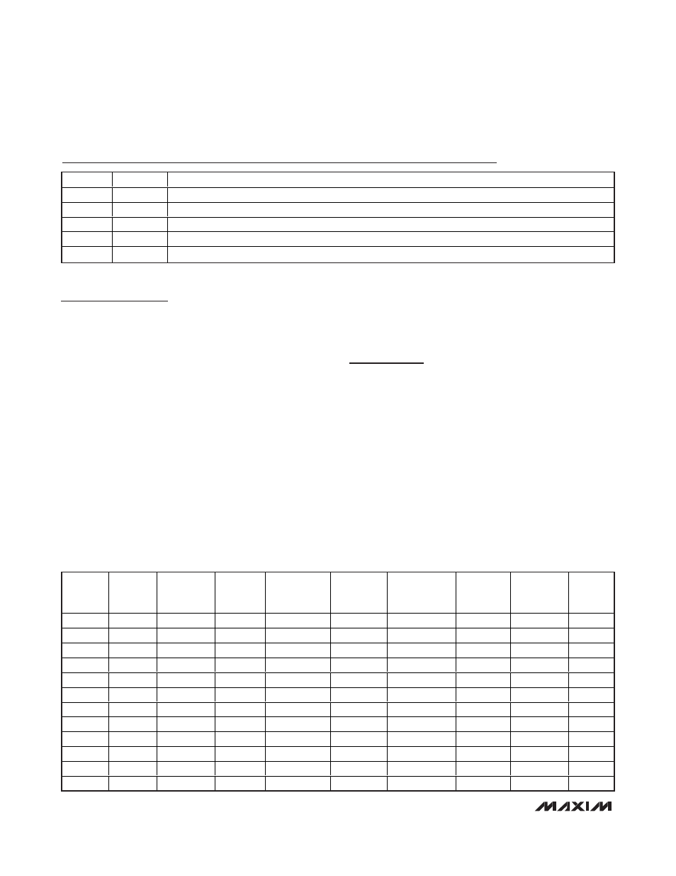
Table 1. MAX2657 Typical S-Parameter Values and K-Factor
FREQ.
(MHz)
S11 MAG
(dB)
S11
PHASE
(Degrees)
S21 MAG
(dB)
S21
PHASE
(Degrees)
S12 MAG
(dB)
S12
PHASE
(Degrees)
S22 MAG
(dB)
S22
PHASE
(Degrees)
K
f
1000
-2.0
-47.7
6.0
-100.0
-47.5
-148.0
-1.0
-55.0
5.1
1100
-2.1
-48.6
7.4
-100.6
-45.7
-150.0
-1.0
-58.1
3.8
1200
-2.2
-51.6
9.6
-107.3
-42.9
-153.5
-1.4
-65.4
3.1
1300
-2.4
-55.0
12.0
-117.2
-39.6
-160.2
-2.1
-74.1
2.5
1400
-2.7
-58.6
14.0
-129.5
-37.0
-168.5
-3.6
-85.5
2.3
1500
-6.5
-61.9
16.2
-146.5
-34.1
178.5
-7.4
-100.0
2.8
1575
-4.3
-62.3
17.1
-164.2
-32.9
162.8
-15.3
-100.8
2.1
1600
-4.6
-61.6
17.3
-170.6
-32.8
156.6
-20.6
-78.9
2.0
1700
-5.4
-55.3
17.1
165.5
-32.5
136.5
-9.5
10.0
1.8
1800
-5.2
-49.8
15.7
145.8
-33.8
121.6
-4.5
-2.4
1.6
1900
-4.8
-47.3
13.9
135.2
-35.2
113.8
-2.7
-13.2
1.6
2000
-4.5
-46.7
12.7
127.3
-36.7
109.6
-1.8
-21.2
1.5
