Rainbow Electronics MAX1669 User Manual
Page 13

GPIO Data Register
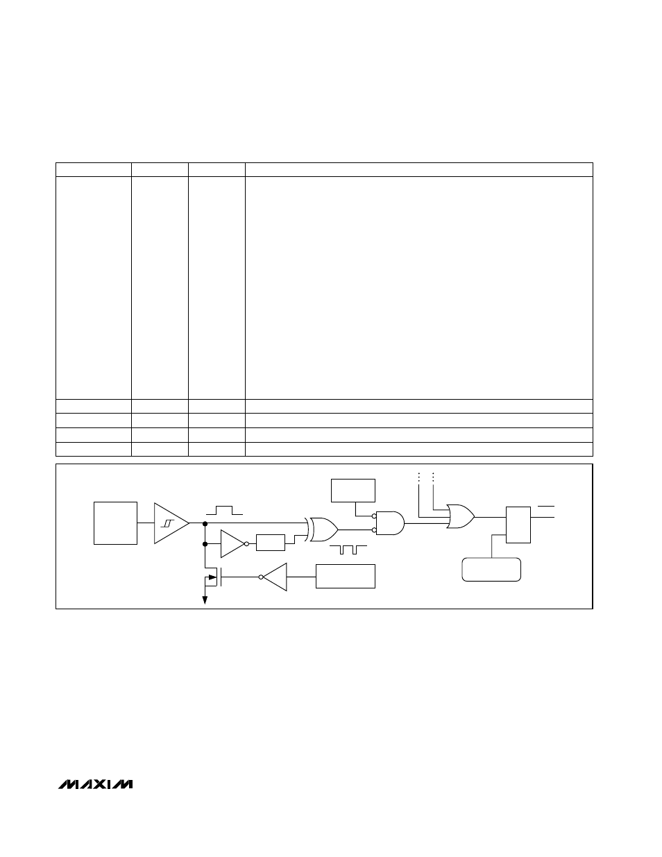
I/O1 and I/O2 are configured through the GPIO data
register and CONFIG byte register (Table 7 and Table 3).
Upon power-up, the GPIOs are set as inputs. To ensure
the I/Os are configured as inputs, set the state of the
DATA1 and DATA2 bits high within the GPIO data reg-
ister for I/O1 and I/O2, respectively. Figure 4 shows that
by setting the GPIO DATA_ bits high, the open-drain
FET connected to the I/O_ pins goes high impedance.
Next, clear the MASK1 and MASK2 bits low within the
CONFIG byte register to remove the masks on the
ALERT interrupts for I/O1 and I/O2, respectively.
To use I/O1 or I/O2 as an output, first set the MASK1
and MASK2 bits high, respectively. Setting the MASK_
bits high within the CONFIG byte register masks out the
corresponding I/O ALERT interrupts. Since the internal
FETs are open-drain, a pull-up resistor is required from
I/O_ to V
CC
. The DATA1 and DATA2 bits within the
GPIO data register directly control the state of the out-
puts of I/O1 and I/O2, respectively (Figure 4).
MAX1669
Fan Controller and Remote Temperature Sensor
with SMBus Serial Interface
______________________________________________________________________________________
13
BIT
NAME
NAME
0
5
D1
FAN duty-factor control bit
0
3–0
RFU
Reserved for future use
0
0
4
0
D0
FAN duty-factor control bit
6
D2
7 (MSB)
D3
FUNCTION
FAN duty-factor control bit
FAN duty-factor control bit. D3–D0 are decoded as follows:
D3–D0
Duty
V
OUT
(nominal)
0000b
0%
0V
0001b
6.67%
0.0625
·
V
CC
0010b
13.33%
0.125
·
V
CC
0011b
20%
0.1875
·
V
CC
0100b
26.67%
0.25
·
V
CC
0101b
33.33%
0.3125
·
V
CC
0110b
40%
0.375
·
V
CC
0111b
46.67%
0.4375
·
V
CC
1000b
53.33%
0.5
·
V
CC
1001b
60%
0.5625
·
V
CC
1010b
66.67%
0.625
·
V
CC
1011b
73.33%
0.6875
·
V
CC
1100b
80%
0.75
·
V
CC
1101b
86.67%
0.8125
·
V
CC
1110b
93.33%
0.875
·
V
CC
1111b
100%
0.9375
·
V
CC
Table 6. Fan Duty-Factor Data Byte Bit Assignments (Write Command = 1Bh)
S
R
ALERT
MASK_ BITS
GPIO DATA_ BITS
DELAY
I/O_ PIN
ALERT RESPONSE
Figure 4. GPIO Logic Diagram
