Rainbow Electronics MAX1200 User Manual
Page 9
MAX1200
+5V Single-Supply, 1Msps, 16-Bit
Self-Calibrating ADC
_______________________________________________________________________________________
9
Choice of Reference
It is important to choose a low-noise reference such as
the MAX6341, which can provide both excellent load
regulation and low temperature drift. The equivalent
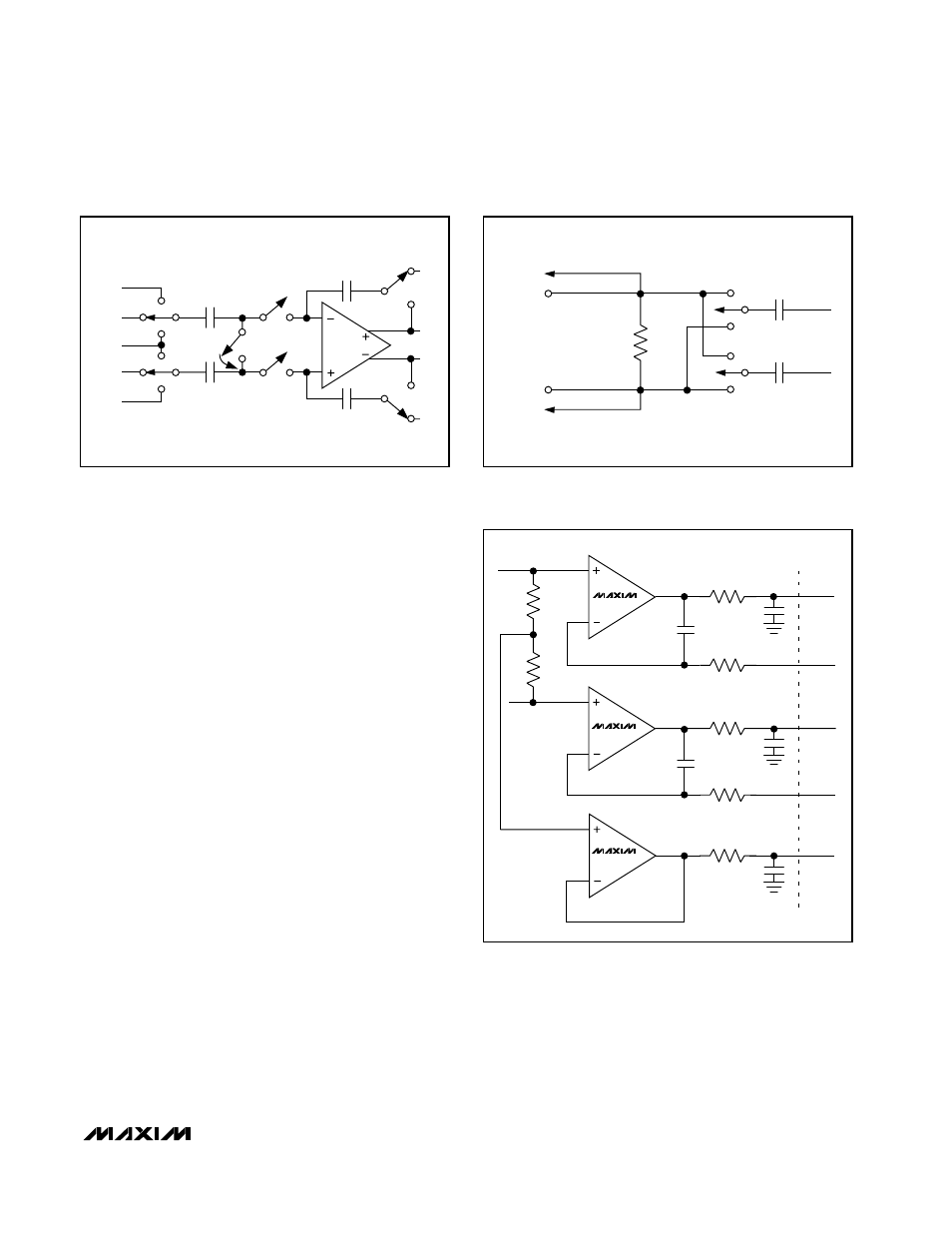
input circuit for the reference pins is shown in Figure 3.
Note that the reference pins drive approximately 1k
Ω
of
resistance on-chip. They also drive a switched capaci-
tor of 21pF. To meet the dynamic performance, the ref-
erence voltage is required to settle to 0.0015% within
one clock cycle. Carefully choose an appropriate driv-
ing circuit (Figure 4). The capacitors at the reference
pins (RFPF, RFNF) provide the dynamic charge
required during each clock cycle, while the op amps
ensure accuracy of the reference signals. These
capacitors must have low dielectric-absorption charac-
teristics, such as polystyrene or teflon capacitors.
The reference pins can be connected to either single-
ended or differential voltages within the specified maxi-
mum levels. Typically the positive reference pin (RFPF)
would be driven to +4.096V, and the negative refer-
ence pin (RFNF) connected to analog ground for best
SNR performance. If THD performance is more impor-
tant to the application than signal-to-noise ratio, choose
a lower level, differential voltage such as V
RFPS
=
+3.5V and V
RFNS
= +1.5V.
There are sense pins, RFPS and RFNS, which can be
used with external amplifiers to compensate for any
resistive drop on these lines, internal or external to the
chip. Ensure a correct reference voltage by using prop-
er Kelvin connections at the sense pins.
Common-Mode Voltage
The switched-capacitor input circuit at the analog input
allows signals between AGND and the analog power
supply. Since the common-mode voltage has a strong
influence on the performance of the ADC, the best
results are obtained by choosing V
CM
= (V
RFPS
+
V
RFNS
) / 2. This can be achieved by using a resistive
divider between the two reference potentials. Figure 4
shows a typical driving circuit for good dynamic perfor-
mance.
RFPF
INP
INN
RFPF
CM
CM
RFNF
Figure 2. Simplified MDAC Architecture
RFPF
RFPS
RFNF
RFNS
Figure 3. Equivalent Input at the Reference Pins. The sense
pins should not draw any DC current.
V
RFP
= +4.096V
V
RFN
= 0
5k
5k
MAX410
CHIP BOUNDARY
CM
RFNS
RFNF
RFPS
RFPF
MAX410
MAX410
Figure 4. Drive Circuit for Reference Pins and Common-Mode
Pin