Digital input and output characteristics, Timing characteristics (figures 7, 8, 9) – Rainbow Electronics MAX1200 User Manual
Page 4
MAX1200
+5V Single-Supply, 1Msps, 16-Bit
Self-Calibrating ADC
4
_______________________________________________________________________________________
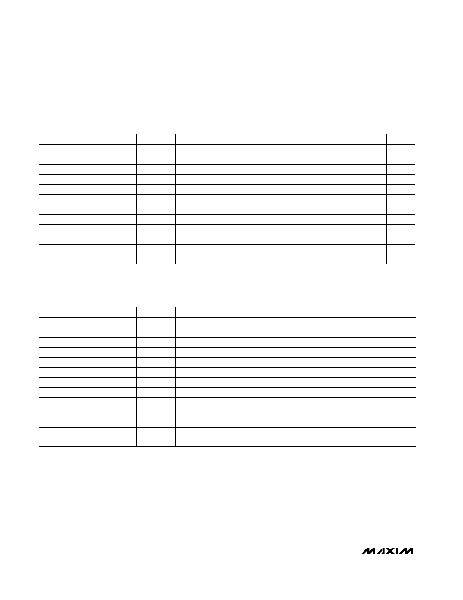
DIGITAL INPUT AND OUTPUT CHARACTERISTICS
(AV
DD
= +5V ±5%, DV
DD
= DRV
DD
= +3.3V, T
A
= T
MIN
to T
MAX
, unless otherwise noted. Typical values are at T
A
= +25°C.)
Note 1:
Reference inputs driven by operational amplifiers for Kelvin-sensed operation.
Note 2:
For unipolar mode, the analog input voltage, V
INP
, must be within 0 and V
REF
, V
INN
= V
CM
/ 2; where V
REF
= V
RFPS
- V
RFNS
.
For differential mode, the analog input voltages V
INP
and V
INN
must be within 0 and V
REF
; where V
REF
= V
RFPS
- V
RFNS
. The
common-mode voltage of the inputs INP and INN is V
CM =
(V
RFPS +
V
RFNS
) / 2.
Note 3:
R
I
varies inversely with sample rate.
Note 4:
Minimum and maximum parameters are not tested. Guaranteed by design.
Note 5:
Calibration remains valid for temperature changes within ±20°C and power-supply variations ±5%. Guaranteed by design.
Note 6:
All AC specifications are shown for the differential mode.
I
SOURCE
= 200µA
V
IN
= 0 or DV
DD
CONDITIONS
4
Input Capacitance
DV
DD
- 0.8
V
IH
0.8
V
IL
Input LOW Voltage
Input HIGH Voltage
DV
DD
DV
DD
- 0.4
- 0.03
V
OH
Output High Voltage
0.8
V
CLK
CLK Input LOW Voltage
AV
DD
- 0.8
V
CLK
CLK Input HIGH Voltage
9
C
CLK
CLK Input Capacitance
±0.1
±10
I
IN
Digital Input Current
MIN
TYP
MAX
SYMBOL
PARAMETER
I
SINK
= 1.6mA
70
400
V
OL
Output Low Voltage
±0.1
±10
I
LEAKAGE
Three-State Leakage Current
3.5
C
OUT
Three-State Output Capacitance
mV
µA
pF
pF
V
V
V
V
V
pF
µA
UNITS
V
IN
= 0 or V
DD
±1
±10
I
CLK
CLK Input Current
µA
C
L
= 20pF
CONDITIONS
ns
187
244
301
t
CH
Clock HIGH Time
ns
488
t
CLK
ns
4 / f
SAMPLE
t
CONV
Conversion Time
Clock Period
ns
16
75
t
REL
Bus Relinquish Time
ns
16
75
t
AC
Data Access Time
ns
187
244
301
t
CL
Clock LOW Time
ns
70
150
t
OD
Output Delay
ns
1 / f
CLK
t
DAV
DAV Pulse Width
ns
65
145
t
S
CLK-to-DAV Rising Edge
UNITS
MIN
TYP
MAX
SYMBOL
PARAMETER
ST_CAL = DV
DD
f
CLK
Cycles
17,400
t
CAL
Calibration Time
ns
t
CLK
/ 2
t
ACQ
Acquisition Time
TIMING CHARACTERISTICS (Figures 7, 8, 9)
(AV
DD
= +5V ±5%, DV
DD
= DRV
DD
= +3.3V, f
CLK
= 2.048MHz, T
A
= T
MIN
to T
MAX
, unless otherwise noted. Typical values are at
T
A
= +25°C.) (Note 1)