Detailed description – Rainbow Electronics MAX1200 User Manual
Page 8
MAX1200
+5V Single-Supply, 1Msps, 16-Bit
Self-Calibrating ADC
8
_______________________________________________________________________________________
Detailed Description
Converter Operation
The MAX1200 is a 16-bit, monolithic analog-to-digital
converter (ADC) capable of conversion rates up to
1Msps. It uses a multistage, fully differential, pipelined
architecture with digital error correction and self-cali-
bration to provide typically 91dB spurious-free dynamic
range at a 1Msps sampling rate. It also provides excel-
lent SNR and THD performance up to the Nyquist fre-
quency. This makes the device suitable for applications
such as data acquisition, high-resolution imaging,
scanners, digital communication, and instrumentation.
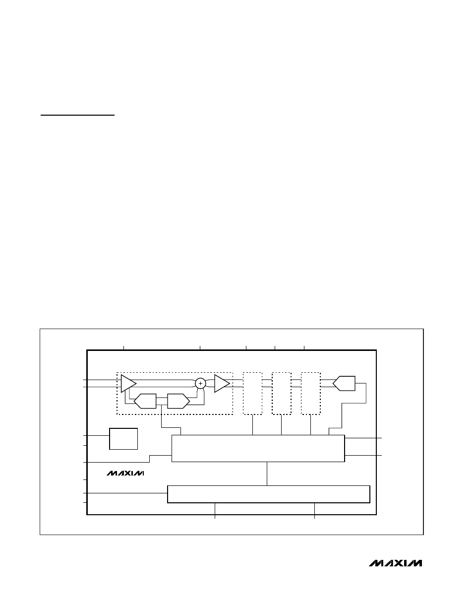
Figure 1 shows the simplified, internal structure of the
ADC. A switched-capacitor, pipelined architecture is
used to digitize the signal at a high throughput rate.
The first four stages of the pipeline use a low-resolution
quantizer to approximate the input signal. The multiply-
ing digital-to-analog converter (MDAC) stage is used to
subtract the quantized analog signal from the input.
The residue is then amplified with a fixed gain and
passed on to the next stage. The accuracy of the con-
verter is improved by a digital calibration algorithm
which corrects for mismatches between the capacitors
in the switched-capacitor MDAC. Note that the pipeline
introduces latency of four sampling periods between
the input being sampled and the output appearing at
D15–D0.
While the device can handle both single-ended or dif-
ferential inputs (see the
Requirements for Reference
and Analog Signal Inputs
section), the latter mode of
operation will guarantee best THD and SFDR perfor-
mance. The differential input provides the following
advantages compared to a single-ended operation:
•
Twice as much signal input span
•
Common-mode noise immunity
•
Virtual elimination of the even-order harmonics
•
Less stringent requirements on the input signal pro-
cessing amplifiers
Requirements for Reference
and Analog Signal Inputs
Fully differential switched-capacitor circuits (SC) are used
for both the reference and analog inputs (Figure 2). This
allows either single-ended or differential signals to be
used in the reference and/or analog signal paths. The
signal voltage on these pins (INP, INN, RFP_, RFN_)
should never exceed the analog supply rail, AV
DD
, nor
fall below ground.
STAGE1
DAV
INP
CM
AV
DD
RFN_
RFP_
AGND
INN
CLK
DV
DD
DGND
DRV
DD
ST_CAL
DOR
D15–D0
ADC
ADC
MDAC
8X
S/H
STAGE2
STAGE3
STAGE4
CORRECTION AND
CALIBRATION LOGIC
END_CAL
OE
OUTPUT DRIVERS
CLOCK
GENERATOR
MAX1200
Figure 1. Internal Functional Diagram