Rainbow Electronics MAX1200 User Manual
Page 2
MAX1200
+5V Single-Supply, 1Msps, 16-Bit
Self-Calibrating ADC
2
_______________________________________________________________________________________
ABSOLUTE MAXIMUM RATINGS
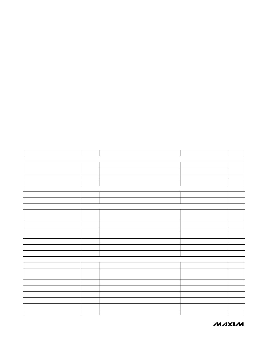
ELECTRICAL CHARACTERISTICS
(AV
DD
= +5V ±5%, DV
DD
= DRV
DD
= +3.3V, V
RFPS
= +4.096V, V
RFNS
= AGND, V
CM
= +2.048V, V
IN
= -0.5dBFS, f
CLK
= 2.048MHz;
digital output load
≤
20pF; T
A
= T
MIN
to T
MAX
, unless otherwise noted. Typical values are at T
A
= +25°C.) (Note 1)
Stresses beyond those listed under “Absolute Maximum Ratings” may cause permanent damage to the device. These are stress ratings only, and functional
operation of the device at these or any other conditions beyond those indicated in the operational sections of the specifications is not implied. Exposure to
absolute maximum rating conditions for extended periods may affect device reliability.
AV
DD
to AGND, DGND ..........................................................+7V
DV
DD
to DGND, AGND..........................................................+7V
DRV
DD
to DGND, AGND .......................................................+7V
INP, INN, RFPF, RFPS,
RFNF, RFNS, CLK, CM..........(AGND - 0.3V) to (AV
DD
+ 0.3V)
Digital Inputs to DGND ............................-0.3V to (DV
DD
+ 0.3V)
Digital Output (DAV) to DGND ..............-0.3V to (DRV
DD
+ 0.3V)
Other Digital Outputs to DGND .............-0.3V to (DRV
DD
+ 0.3V)
Continuous Power Dissipation (T
A
= +70°C)
44-Pin MQFP (derate 11.11mW/°C above +70°C).......889mW
Operating Temperature Ranges (T
A
)
MAX1200_CMH ..................................................0°C to +70°C
MAX1200_EMH................................................-40°C to +85°C
Storage Temperature Range .............................-65°C to +150°C
Lead Temperature (soldering, 10sec) .............................+300°C
To full-scale step (0.006%)
ns
3
t
AD
Aperture Delay
ns
450
t
OVR
ns
125
t
ACQ
Acquisition Time
Overvoltage Recovery Time
MHz
3.3
MHz
78
Small-Signal Bandwidth
MAX1200A
After calibration, guaranteed for
MAX1200A only
f
SAMPLE =
f
CLK /
2
LSB
-1
±0.5
+1
DNL
Differential Nonlinearity
LSB
±3.5
INL
Bits
16
RES
Resolution
(No missing codes; Note 5)
Integral Nonlinearity
f
SAMPLE
Cycles
4
Conversion Time
(Pipeline Delay/Latency)
Msps
1.024
f
SAMPLE
Maximum Sampling Rate
%FSR
-0.2
±0.003
+0.2
Offset Error
%FSR
-5
-3
5
Gain Error
µV
RMS
75
Input-Referred Noise
Differential
Single-ended
Per side in track mode
CONDITIONS
±4.096
V
4.096
V
IN
Input Voltage Range (Note 2)
Ω
700
1000
R
REF
Reference Input Resistance
k
Ω
55
R
I
Input Resistance (Note 3)
pF
21
C
I
Input Capacitance
V
4.096
4.5
V
REF
Reference Voltage (Note 4)
UNITS
MIN
TYP
MAX
SYMBOL
PARAMETER
Full-Power Bandwidth
ps
RMS
5
t
AJ
Aperture Jitter
ANALOG INPUT
EXTERNAL REFERENCE
TRANSFER CHARACTERISTICS
DYNAMIC SPECIFICATIONS
(Note 6)
MAX1200B
±0.6