Rainbow Electronics MAX669 User Manual
Page 9
PWM Controller
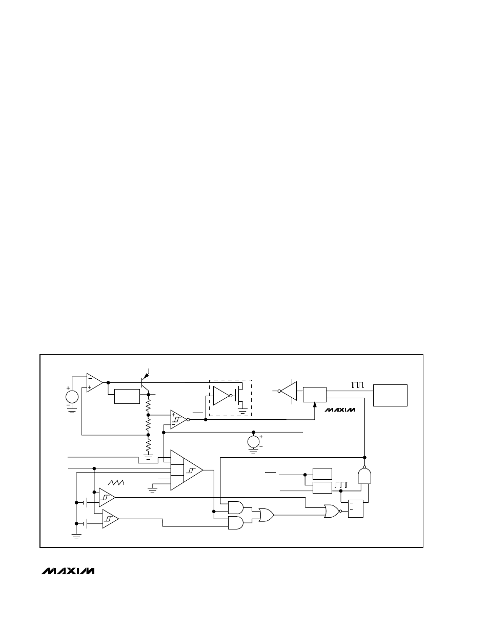
The heart of the MAX668/MAX669 current-mode PWM
controller is a BiCMOS multi-input comparator that
simultaneously processes the output-error signal, the
current-sense signal, and a slope-compensation ramp
(Figure 1). The main PWM comparator is direct sum-
ming, lacking a traditional error amplifier and its associ-
ated phase shift. The direct summing configuration
approaches ideal cycle-by-cycle control over the out-
put voltage since there is no conventional error amp in
the feedback path.
In PWM mode, the controller uses fixed-frequency, cur-
rent-mode operation where the duty ratio is set by the
input/output voltage ratio (duty ratio = (V
OUT
- V
IN
) / V
IN
in the boost configuration). The current-mode feedback
loop regulates peak inductor current as a function of
the output error signal.
At light loads the controller enters Idle Mode. During
Idle Mode, switching pulses are provided only as need-
ed to service the load, and operating current is mini-
mized to provide best light-load efficiency. The
minimum-current comparator threshold is 15mV, or 15%
of the full-load value (I
MAX
) of 100mV. When the con-
troller is synchronized to an external clock, Idle Mode
occurs only at very light loads.
Bootstrapped/Non-Bootstrapped Operation
Low-Dropout Regulator (LDO)
Several IC biasing options, including bootstrapped and
non-bootstrapped operation, are made possible by an
on-chip, low-dropout 5V regulator. The regulator input is
at V
CC
, while its output is at LDO. All MAX668/MAX669
functions, including EXT, are internally powered from
LDO. The V
CC
-to-LDO dropout voltage is typically
200mV (300mV max at 12mA), so that when V
CC
is less
than 5.2V, LDO is typically V
CC
- 200mV. When LDO is
in dropout, the MAX668/MAX669 still operate with V
CC
as low as 3V (as long as LDO exceeds 2.7V), but with
reduced amplitude FET drive at EXT. The maximum
V
CC
input voltage is 28V.
LDO can supply up to 12mA to power the IC, supply
gate charge through EXT to the external FET, and sup-
ply small external loads. When driving particularly large
FETs at high switching rates, little or no LDO current
may be available for external loads. For example, when
switched at 500kHz, a large FET with 20nC gate charge
requires 20nC x 500kHz, or 10mA.
V
CC
and LDO allow a variety of biasing connections to
optimize efficiency, circuit quiescent current, and full-
load start-up behavior for different input and output
voltage ranges. Connections are shown in Figures 2, 3,
4, and 5. The characteristics of each are outlined in
Table 1.
MAX668/MAX669
1.8V to 28V Input, PWM Step-Up
Controllers in µMAX
_______________________________________________________________________________________
9
ANTISAT
MUX
LOW-VOLTAGE
START-UP
OSCILLATOR
(MAX669 ONLY)
+A
-A X6
+C
-C X1
+S
-S
X1
SLOPE COMPENSATION
S Q
BIAS
OSC
OSC
FREQ
SYNC/SHDN
0
1
LDO
PGND
1.25V
REF
EXT
UVLO
V
CC
R1
552k
R2
276k
R3
276k
100mV
15mV
I
MAX
I
MIN
MAIN PWM
COMPARATOR
1.25V
FB
CURRENT SENSE
CS+
MAX668
MAX669
LDO
MAX669 ONLY
R
Figure 1. MAX668/MAX669 Functional Diagram