Rainbow Electronics MAX669 User Manual
Page 10
MAX668/MAX669
1.8V to 28V Input, PWM Step-Up
Controllers in µMAX
10
______________________________________________________________________________________
MAX669
LDO
CS+
REF
FREQ
V
CC
SYNC/
SHDN
PGND
FB
GND
N1
EXT
V
IN
= 1.8V to 12V
C3
0.22
µ
F
C2
0.1
µ
F
C4
1
µ
F
R4
100k
1%
R1
0.02
Ω
R2
218k
1%
R3
24.9k
1%
C7
220pF
D1
MBRS340T3
C5
68
µ
F
20V
C6
68
µ
F
20V
C8
0.1
µ
F
3
5
7
6
8
2
4
9
1
10
V
OUT
= 12V @ 0.5A
C1
68
µ
F
20V
L1
4.7
µ
H
IRF7401
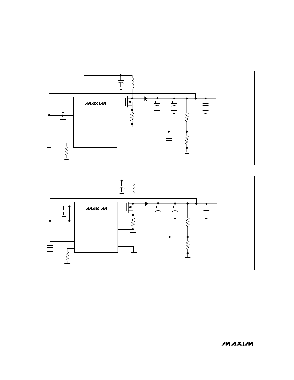
Figure 2. MAX669 High-Voltage Bootstrapped Configuration
MAX669
LDO
CS+
REF
FREQ
V
CC
SYNC/
SHDN
PGND
FB
GND
N1
EXT
V
IN
= 1.8V to 5V
C3
0.22
µ
F
C2
1
µ
F
R4
100k
1%
R1
0.02
Ω
R2
75k
1%
R3
24.9k
1%
C7
220pF
D1
MBRS340T3
C4
68
µ
F
10V
C5
68
µ
F
10V
C6
0.1
µ
F
3
5
7
6
8
2
4
9
1
10
V
OUT
= 5V @ 1A
C1
68
µ
F
10V
L1
4.7
µ
H
FDS6680
IRF7401
Figure 3. MAX669 Low-Voltage Bootstrapped Configuration
Bootstrapped Operation
With bootstrapped operation, the IC is powered from
the circuit output (V
OUT
). This improves efficiency
when the input voltage is low, since EXT drives the FET
with a higher gate voltage than would be available from
the low-voltage input. Higher gate voltage reduces the
FET on-resistance, increasing efficiency. Other (unde-
sirable) characteristics of bootstrapped operation are
increased IC operating power (since it has a higher
operating voltage) and reduced ability to start up with
high load current at low input voltages. If the input volt-
age range extends below 2.7V, then bootstrapped
operation with the MAX669 is the only option.
With V
CC
connected to V
OUT
, as in Figure 2, EXT volt-
age swing is 5V when V
CC
is 5.2V or more, and V
CC
-
0.2V when V
CC
is less than 5.2V. If the output voltage
does not exceed 5.5V, the on-chip regulator can be
disabled by connecting V
CC
to LDO (Figure 3). This
eliminates the LDO forward drop and supplies maxi-
mum gate drive to the external FET.