8v to 28v input, pwm step-up controllers in µmax – Rainbow Electronics MAX669 User Manual
Page 16
MAX668/MAX669
larger or smaller than the output voltage, such as when
converting four NiMH, NiCd, or Alkaline cells to a 5V
output. The SEPIC configuration is often a good choice
for combined step-up/step-down applications.
The N-channel MOSFET (Q1) must be selected to with-
stand a drain-to-source voltage (V
DS
) greater than the
sum of the input and output voltages. The coupling
capacitor (C2) must be a low-ESR type to achieve max-
imum efficiency. C2 must also be able to handle high
ripple currents; ordinary tantalum capacitors should not
be used for high-current designs.
The circuit in Figure 6 provides greater than 1A output
current at 5V when operating with an input voltage from
3V to 25V. Efficiency will typically be between 70% and
85%, depending upon the input voltage and output cur-
rent.
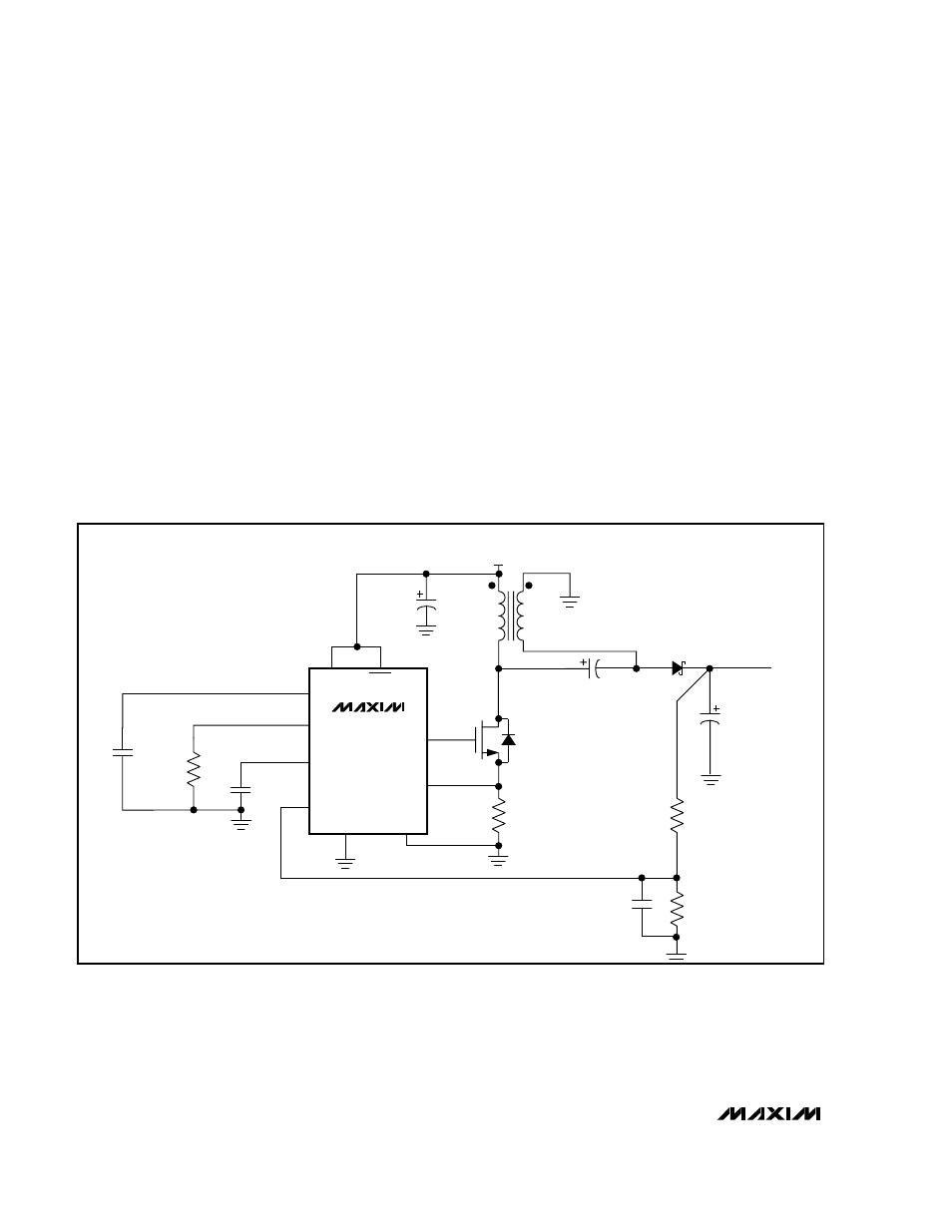
Isolated +5V to +5V Power Supply
The circuit of Figure 7 provides a 5V isolated output at
400mA from a 5V input power supply. Transformer T1
provides electrical isolation for the forward path of the
converter, while the TLV431 shunt regulator and
MOC211 opto-isolator provide an isolated feedback
error voltage for the converter. The output voltage is set
by resistors R2 and R3 such that the mid-point of the
divider is 1.24V (threshold of TLV431). Output voltage
can be adjusted from 1.24V to 6V by selecting the
proper ratio for R2 and R3. For output voltages greater
than 6V, substitute the TL431 for the TLV431, and use
2.5V as the voltage at the midpoint of the voltage-
divider.
1.8V to 28V Input, PWM Step-Up
Controllers in µMAX
16
______________________________________________________________________________________
R3
100k
R4
0.02
Ω
R1
75k
R2
25k
C4
520pF
V
IN
3V to 25V
30V
FDS6680
Q1
L1
CTX5-4
MAX668
SHDN
VCC
9
10
LDO
FREQ
D1: MBR5340T3, 3A, 40V SCHOTTKY DIODE
R4: WSL-2512-R020F, 0.02
Ω
C3: AVX TPSZ686M020R0150, 68
µ
F, 150m
Ω
ESR
REF
EXT
CS+
8
6
PGND
GND
7
3
FB
1
2
4
5
1
µ
F
22
µ
F x 3
@ 35V
C3
68
µ
F x 3
V
OUT
5V @ 1A
4.9
µ
H
C2
10
µ
F @ 35V
D1
40V
0.22
µ
F
Figure 6. MAX668 in SEPIC Configuration