Detailed description, Pin description – Rainbow Electronics MAX669 User Manual
Page 8
Detailed Description
The MAX668/MAX669 current-mode PWM controllers
operate in a wide range of DC-DC conversion applica-
tions, including boost, SEPIC, flyback, and isolated out-
put configurations. Optimum conversion efficiency is
maintained over a wide range of loads by employing
both PWM operation and Maxim’s proprietary Idle
Mode control to minimize operating current at light
loads. Other features include shutdown, adjustable
internal operating frequency or synchronization to an
external clock, soft start, adjustable current limit, and a
wide (1.8V to 28V) input range.
MAX668 vs. MAX669 Differences
Differences between the MAX668 and MAX669 relate
to their use in bootstrapped or non-bootstrapped cir-
cuits (Table 1). The MAX668 operates with inputs as
low as 3V and can be connected in
either a boot-
strapped or non-bootstrapped (IC powered from input
supply or other source) configuration. When not boot-
strapped, the MAX668 has no restriction on output volt-
age. When bootstrapped, the output cannot exceed
28V.
The MAX669 is optimized for low input voltages (down
to 1.8V) and
requires bootstrapped operation (IC pow-
ered from V
OUT
) with output voltages no greater than
28V. Bootstrapping is required because the MAX669
does not have undervoltage lockout, but instead drives
EXT with an open-loop, 50% duty-cycle start-up oscilla-
tor when LDO is below 2.5V. It switches to closed-loop
operation only when LDO exceeds 2.5V. If a non-boot-
strapped connection is used with the MAX669 and if
V
CC
(the input voltage) remains below 2.7V, the output
voltage will soar above the regulation point. Table 2
recommends the appropriate device for each biasing
option.
MAX668/MAX669
1.8V to 28V Input, PWM Step-Up
Controllers in µMAX
8
_______________________________________________________________________________________
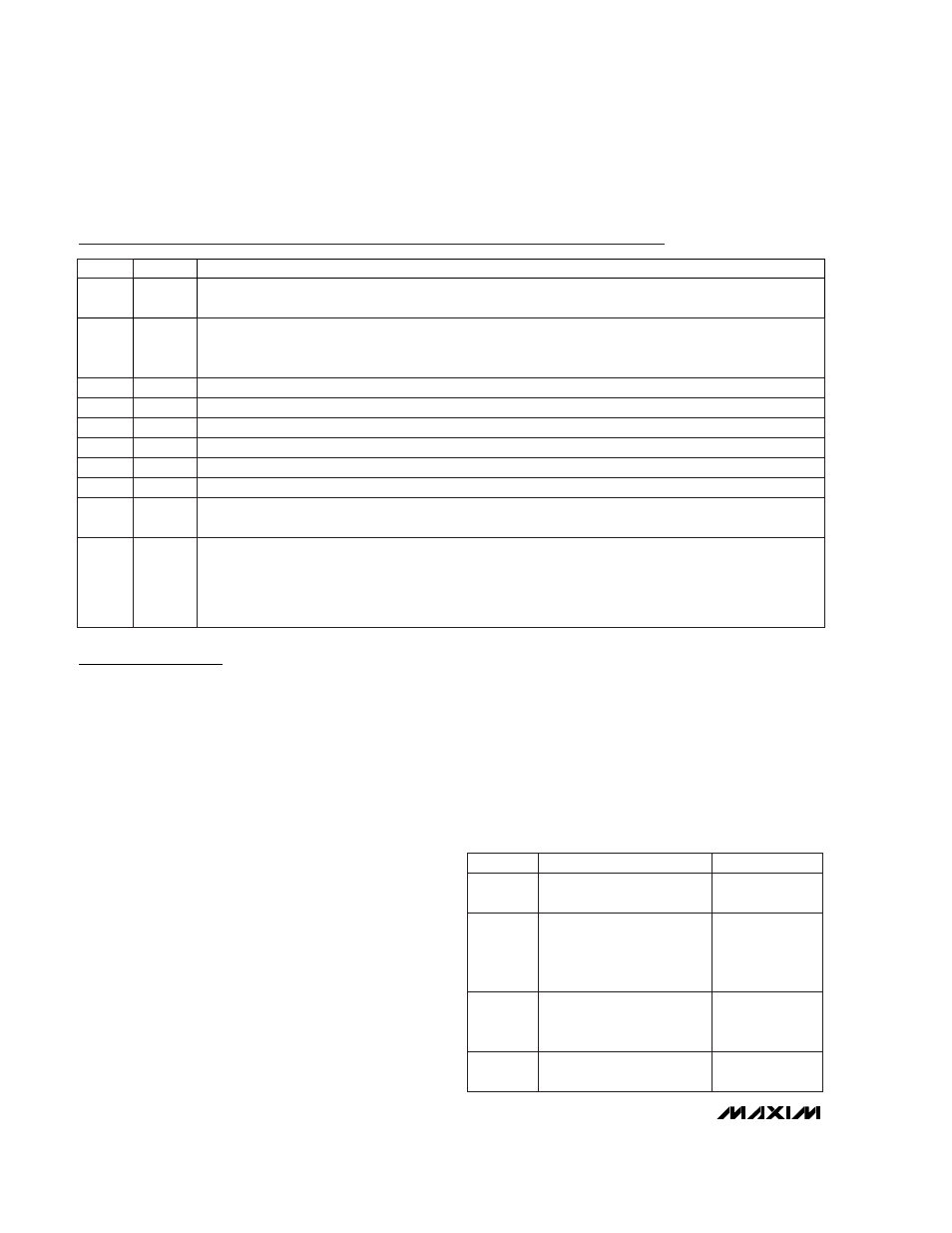
NAME
FUNCTION
1
LDO
5V On-Chip Regulator Output. This regulator powers all internal circuitry including the EXT gate driver.
Bypass LDO to GND with a 1µF or greater ceramic capacitor.
2
FREQ
Oscillator Frequency Set Input. A resistor from FREQ to GND sets the oscillator from 100kHz (R
OSC
=
500k
Ω
) to 500kHz (R
OSC
= 100k
Ω
). f
OSC
= 5 x 10
10
/ R
OSC
. R
OSC
is still required if an external clock is used
at SYNC/SHDN. (See
SYNC/
SHDN and FREQ Inputs section.)
PIN
3
GND
Analog Ground
7
PGND
Power Ground for EXT Gate Driver and Negative Current-Sense Input
6
CS+
Positive Current-Sense Input. Connect a current-sense resistor, R
CS
, between CS+ and PGND.
5
FB
Feedback Input. The FB threshold is 1.25V.
4
REF
1.25V Reference Output. REF can source 50µA. Bypass to GND with a 0.22µF ceramic capacitor.
10
SYNC/
SHDN
Shutdown control and Synchronization Input. There are three operating modes:
• SYNC/SHDN low: DC-DC off.
• SYNC/SHDN high: DC-DC on with oscillator frequency set at FREQ by R
OSC
.
• SYNC/SHDN clocked: DC-DC on with operating frequency set by SYNC clock input. DC-DC conversion
cycles initiate on rising edge of input clock.
9
V
CC
Input Supply to On-Chip LDO Regulator. V
CC
accepts inputs up to 28V. Bypass to GND with a 0.1µF ceramic
capacitor.
8
EXT
External MOSFET Gate-Driver Output. EXT swings from LDO to PGND.
Pin Description
Table 1. MAX668/MAX669 Comparison
MAX668
MAX669
V
CC
Input
Range
3V to 28V
1.8V to 28V
Operation
Bootstrapped or nonboot-
strapped. V
CC
can be con-
nected to input, output, or
other voltage source such as
a logic supply.
Must be boot-
strapped (V
CC
must be connect-
ed to boosted out-
put voltage, V
OUT
).
Under-
voltage
Lockout
IC stops switching for LDO
below 2.5V.
No
Soft-Start
Yes
When LDO is
above 2.5V
FEATURE