Pin description – Rainbow Electronics MAX1611 User Manual
Page 6
MAX1610/MAX1611
Digitally Controlled CCFL Backlight
Power Supplies
6
_______________________________________________________________________________________
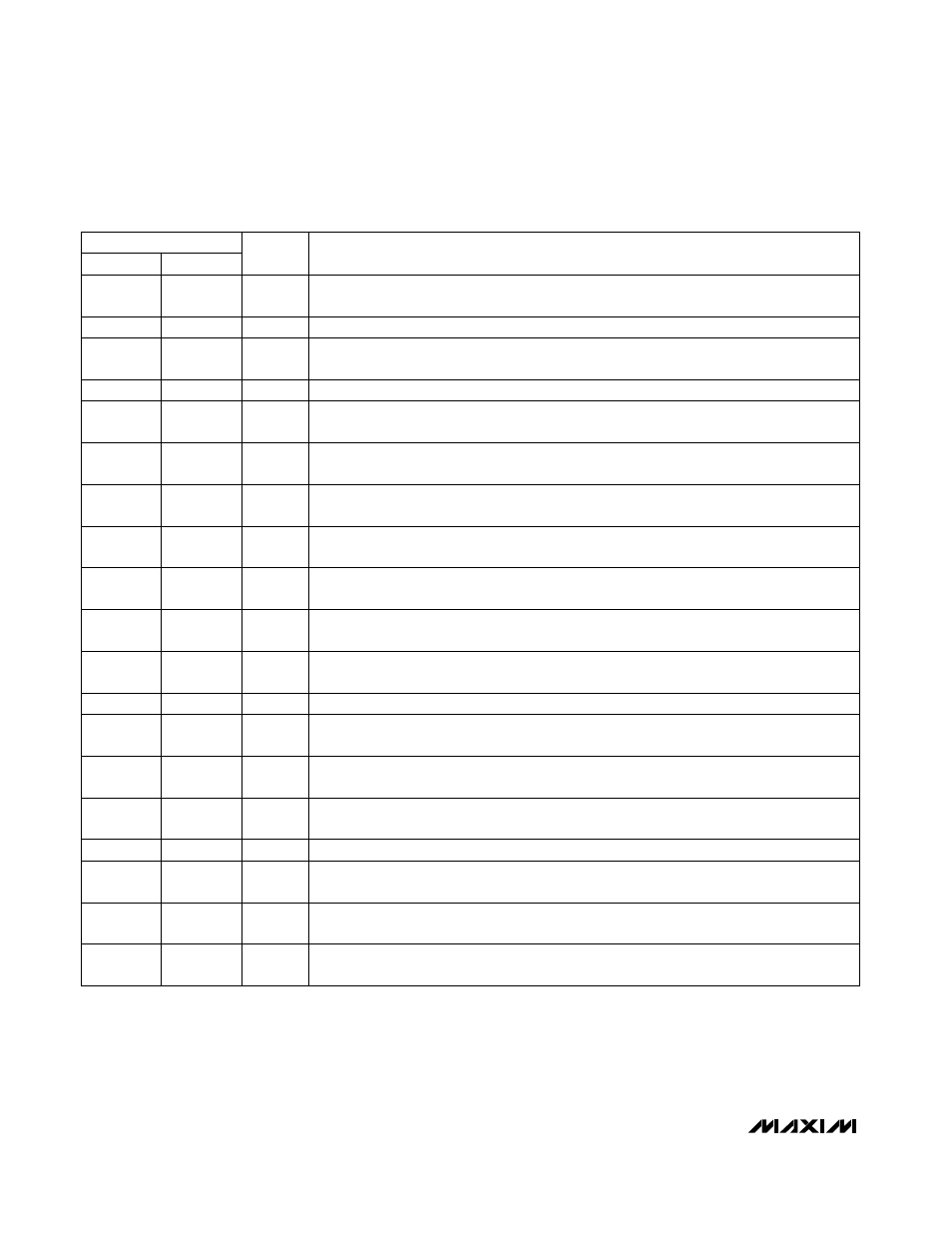
MAX1610
MAX1611
NAME
1
—
UP
PIN
—
1
SDA
2
—
DN
8
8
MINDAC
7
7
CSAV
6
6
CC
—
2
SCL
13
13
GND
12
12
VL
11
11
CS
10
10
OTP
9
9
REF
FUNCTION
Logic-Level Input. A rising edge on UP increments the 5-bit counter for the 5-bit DAC.
UP = DN = 1 presets the counter to mid-scale.
System Management Bus Serial Data Input and Open-Drain Output
Logic-Level Input. A rising edge on DN decrements the 5-bit counter for the 5-bit DAC.
UP = DN = 1 presets the counter to mid-scale.
The voltage at MINDAC sets the DAC’s minimum-scale output voltage. Tying MINDAC to
VL enables the internal 280Hz current-chopping mode.
Input to the Voltage-to-Current Converter, which averages the voltage on CSAV using the
capacitor on CC.
Output of the Voltage-to-Current Converter; Input to the PWM Comparator, which sets the
current limit. A capacitor placed at CC sets the current-regulator-loop bandwidth.
System Management Bus Serial Clock Input
System Ground
Output of the Internal Linear Regulator. VL can be overdriven by a voltage greater than 4.75V
to operate the chip from +5V ± 5%, and to conserve power. Bypass with 0.1
µ
F to GND.
Low-Side Current-Sense Input. The current-mode regulator terminates the switch cycle
when the voltage at CS exceeds REF - CC.
Open-Tube Protection Comparator. As long as OTP exceeds the reference voltage, the
N-channel BATT-to-LX switch is forced off.
2.0V Reference Output. Bypass with 0.1
µ
F to GND.
______________________________________________________________Pin Description
14
14
BST
Power Input to the High-Side Gate Driver, which switches the internal N-channel MOSFET
on and off.
15
15
LX
Ground Connection for the Internal High-Side Gate Driver; source-connection point for the
internal N-channel MOSFET
16
16
BATT
4.5V to 25V Battery-Voltage Input Point. Connects to the internal N-channel power MOSFET’s
drain, and to the input of the internal linear regulator that powers the chip.
3
—
SHDN
—
3
SMBSUS
4
4
SYNC
5
5
SS
Logic-Level Shutdown Input Pin. Applying a logic low to
SHDN places the chip in a low-
supply-current shutdown mode.
System Management Bus Suspend Mode Input. SMBSUS Selects one of two chip-
configuration settings, which are preprogrammed serially.
Oscillator Synchronization Input. Tying SYNC to REF sets the oscillator frequency to 290kHz.
Tying SYNC to GND or VL lowers the oscillator frequency to 145kHz.
Soft-Start Pin. A 4µA current source feeds the capacitor placed on SS. The voltage on this
pin limits the peak current in the switch. When the lamp is turned off, SS pulls to GND.