Detailed description – Rainbow Electronics MAX944 User Manual
Page 7
_______________Detailed Description
The MAX941/MAX942/MAX944 single-supply compara-
tors feature internal hysteresis, high speed, and low
power. Their outputs are guaranteed to pull within 0.4V
of either supply rail without external pullup or pulldown
circuitry. Rail-to-rail input voltage range and low-volt-
age single-supply operation make these devices ideal
for portable equipment. The MAX941/MAX942/
MAX944 interface directly to CMOS and TTL logic.
Timing
Most high-speed comparators oscillate in the linear
region because of noise or undesired parasitic feed-
back. This tends to occur when the voltage on one
input is at or equal to the voltage on the other input. To
counter the parasitic effects and noise, the MAX941/
MAX942/MAX944 have internal hysteresis.
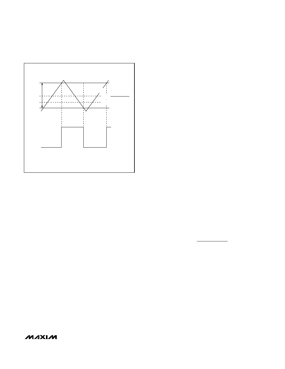
The hysteresis in a comparator creates two trip points:
one for the rising input voltage and one for the falling
input voltage (Figure 1). The difference between the trip
points is the hysteresis. When the comparator’s input
voltages are equal, the hysteresis effectively causes
one comparator input voltage to move quickly past the
other, thus taking the input out of the region where
oscillation occurs. Standard comparators require hys-
teresis to be added with external resistors. The
MAX941/MAX942/MAX944’s fixed internal hysteresis
eliminates these resistors and the equations needed to
determine appropriate values.
Figure 1 illustrates the case where IN- is fixed and IN+
is varied. If the inputs were reversed, the figure would
look the same, except the output would be inverted.
The MAX941 includes an internal latch that allows stor-
age of comparison results. The
L
—
A
—
T
—
C
—
H
–
pin has a high
input impedance. If
L
—
A
—
T
—
C
—
H
–
is high, the latch is transpar-
ent (i.e., the comparator operates as though the latch is
not present). The comparator's output state is stored
when
L
—
A
—
T
—
C
—
H
–
is pulled low. All timing constraints must
be met when using the latch function (Figure 2).
Shutdown Mode (MAX941 Only)
The MAX941 shuts down when
–
S
—
H
—
D
—
N
–
is low. When shut
down, the supply current drops to less than 60µA, and
the three-state output becomes high impedance. The
–
S
—
H
—
D
—
N
–
pin has a high input impedance. Connect
–
S
—
H
—
D
—
N
–
to V+ for normal operation. Exit shutdown with
L
—
A
—
T
—
C
—
H
–
high; otherwise, the output will be indeterminate.
Input Stage Circuitry
The MAX941/MAX942/MAX944 include internal protec-
tion circuitry that prevents damage to the precision
input stage from large differential input voltages. This
protection circuitry consists of two back-to-back diodes
between IN+ and IN- as well as two 4.1k
Ω resistors
(Figure 3). The diodes limit the differential voltage
applied to the internal circuitry of the comparators to be
no more than 2V
F
, where V
F
is the forward voltage drop
of the diode (about 0.7V at +25°C).
For a large differential input voltage (exceeding 2V
F
),
this protection circuitry increases the input bias current
at IN+ (source) and IN- (sink).
Input Current =
(IN+ - IN-) - 2V
F
2 x 4.1k
Ω
Input current with large differential input voltages
should not be confused with input bias current (I
B
). As
long as the differential input voltage is less than 2V
F
,
this input current is equal to I
B
. The protection circuitry
also allows for the input common-mode range of the
MAX941/MAX942/MAX944 to extend beyond both
power-supply rails. The output is in the correct logic
state if one or both inputs are within the common-mode
range.
MAX941/MAX942/MAX944
High-Speed, Low-Power, 3V/5V, Rail-to-Rail,
Single-Supply Comparators
_______________________________________________________________________________________
7
V
TRIP+
V
HYST
V
TRIP-
COMPARATOR
OUTPUT
V
OH
V
OL
V
TRIP+
+ V
TRIP-
2
V
OS
=
V
IN-
= 0
V
IN+
Figure 1. Input and Output Waveform, Noninverting Input
Varied