Electrical characteristics (continued) – Rainbow Electronics MAX944 User Manual
Page 3
MAX941/MAX942/MAX944
High-Speed, Low-Power, 3V/5V, Rail-to-Rail,
Single-Supply Comparators
_______________________________________________________________________________________
3
ELECTRICAL CHARACTERISTICS (continued)
(V+ = 2.7V to 6.0V, T
A
= T
MIN
to T
MAX
, unless otherwise noted. Typical values are at T
A
= +25°C.) (Note 14)
Note 1:
Inferred from the CMRR test. Note also that either or both inputs can be driven to the absolute maximum limit (0.3V
beyond either supply rail) without damage or false output inversion.
Note 2:
The input-referred trip points are the extremities of the differential input voltage required to make the comparator output
change state. The difference between the upper and lower trip points is equal to the width of the input-referred hysteresis
zone (see Figure 1).
Note 3:
V
OS
is defined as the center of the input-referred hysteresis zone (see Figure 1).
Note 4:
The polarity of I
B
reverses direction as V
CM
approaches either supply rail. See Typical Operating Characteristics for more
detail.
Note 5:
Specified over the full common-mode range (V
CMR
).
Note 6:
Applies to the MAX941 only when in shutdown mode. Specification is for current flowing into or out of the output pin for
V
OUT
driven to any voltage from V+ to GND.
Note 7:
Typical power dissipation specified with V+ = 3V; maximum with V+ = 6V.
Note 8:
Parameter is guaranteed by design and specified with V
OD
= 5mV and C
LOAD
= 15pF in parallel with 400µA of sink or
source current. V
OS
is added to the overdrive voltage for low values of overdrive (see Figure 2).
Note 9:
Specified between any two channels in the MAX942/MAX944.
Note 10: Specified as the difference between t
PD+
and t
PD-
for any one comparator.
Note 11: Applies to the MAX941 only for both
–
S
—
H
—
D
—
N
–
and
–
L
—
A
—
T
—
C
—
H
–
pins.
Note 12: Applies to the MAX941 only. Comparator is active with
–
L
—
A
—
T
—
C
—
H
–
pin driven high and is latched with
–
L
—
A
—
T
—
C
—
H
–
pin driven low
(see Figure 2).
Note 13: Applicable to the MAX941 only. Comparator is active with
–
S
—
H
—
D
—
N
–
pin driven high and is in shutdown with
–
S
—
H
—
D
—
N
–
pin driven
low. Shutdown disable time is the delay when
–
S
—
H
—
D
—
N
–
is driven high to the time the output is valid.
Note 14: The MAX941EUA and MAX942EUA are 100% production tested at T
A
= +25°C. Specifications over temperature are
guaranteed by design.
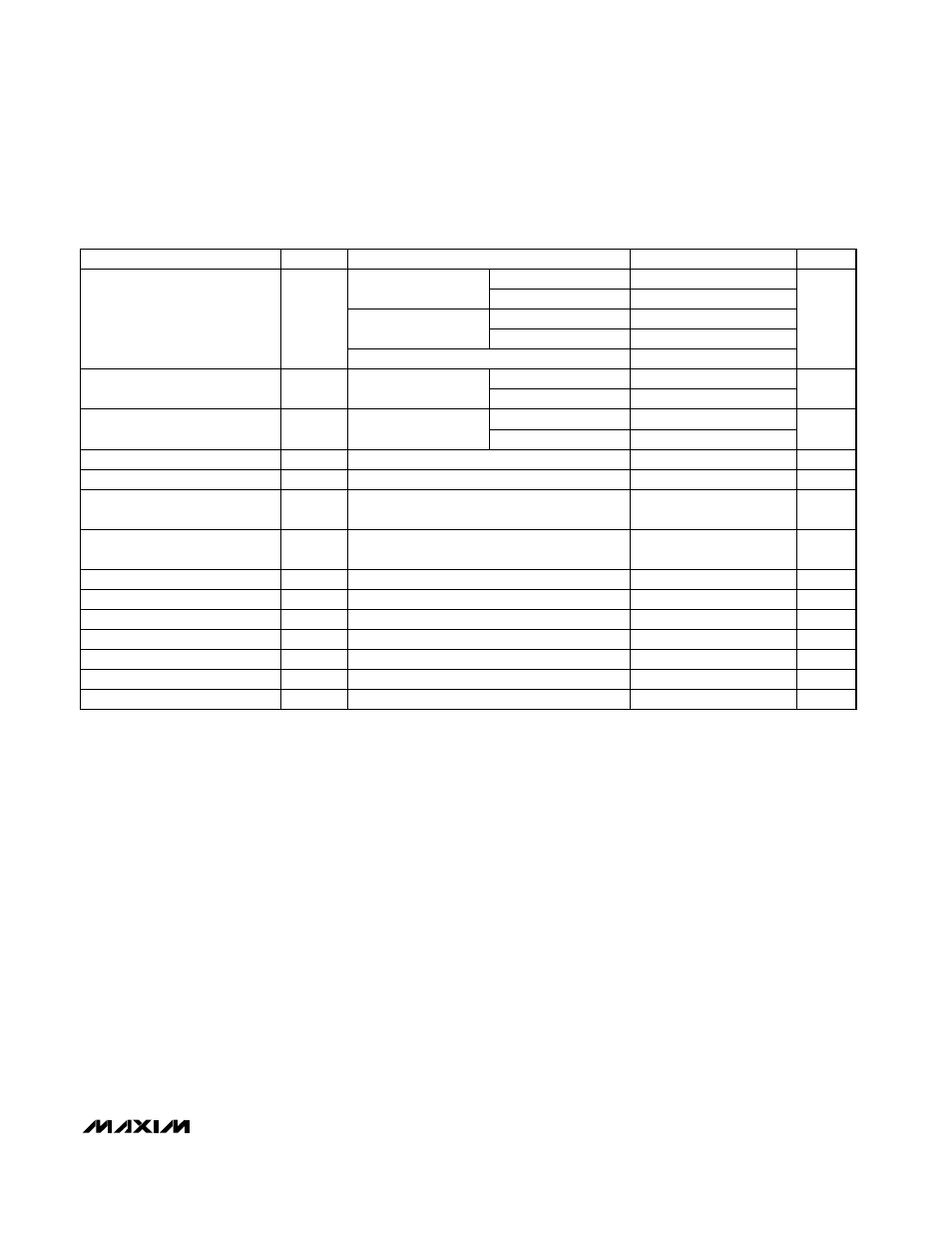
PARAMETER
SYMBOL
CONDITIONS
MIN
TYP
MAX
UNITS
Supply Current per Comparator
380
600
Logic Input Voltage High
V
IH
(Note 11)
–
V
–
2
–
+
–
+ 0.4
–
V
–
2
–
+
–
V
Logic Input Voltage Low
V
IL
(Note 11)
–
V
–
2
–
+
–
–
V
–
2
–
+
–
- 0.4
V
Logic Input Current
I
IL
, I
IH
V
LOGIC
= 0 or V+ (Note 11)
2
10
µA
Data-to-Latch Setup Time
t
S
(Note 12)
20
ns
Latch-to-Data Hold Time
t
H
(Note 12)
30
ns
Latch Pulse Width
t
LPW
MAX941 only
50
ns
Latch Propagation Delay
t
LPD
MAX941 only
70
ns
Shutdown Time
(Note 13)
3
µs
Shutdown Disable Time
(Note 13)
10
µs
Propagation Delay Skew
(Note 10)
10
ns
I
CC
V+ = 3V
350
500
MAX941 only, shutdown mode (V+ = 3V)
12
60
µA
1.0
4.2
Power Dissipation per
Comparator
PD
(Note 7)
1.0
3.6
mW
Differential Propagation Delay
dt
PD
(Note 9)
10
ns
MAX941
MAX942/MAX944
430
700
MAX941
V+ = 5V
400
600
MAX942/MAX944
MAX941
MAX942/MAX944
MAX94_C
MAX94_E
80
150
Propagation Delay
t
PD+
,
t
PD-
(Note 8)
80
200
ns