Pin description, Typical operating characteristics (continued) – Rainbow Electronics MAX1765 User Manual
Page 9
MAX1765
800mA, Low-Noise, Step-Up DC-DC Converter
with 500mA Linear Regulator
_______________________________________________________________________________________
9
PIN
NAME
FUNCTION
1
FBL
Low-Dropout Linear Regulator Dual-Mode Feedback Input. Connect FBL to ground for 2.85V
nominal output voltage. Connect FBL to a resistor-divider from OUTL to ground for an adjustable
output voltage. FBL regulates to 1.25V.
2
ISET
Set N-Channel Current Limit. For maximum current limit, connect ISET to REF. To reduce current
limit, use a resistor-divider from REF to GND. If soft-start is desired, a capacitor can be added from
ISET to GND. When ONA = LO and ONB = HI or V
REF
< 80% of nominal value, an on-chip 100k
Ω
switchable resistor discharges ISET to GND.
3
REF
1.25V Reference Output. Connect a 0.22
µF bypass capacitor to GND; 50µA of external load current
is allowed. The reference is enabled if ONA = HI, ONB = LO, or ONL = HI.
4
GND
Ground. Connect to PGND with short trace.
5
FB
Boost Converter Feedback Input. Connect a resistor-divider between OUT and GND to set the
output voltage in the range of 2.5V to 5V. In track mode, FB is disabled after OUTL is in regulation.
6
OUT
Boost Converter IC power is derived from OUT. Connect OUT to POUT through a 4.7
Ω resistor and
bypass to GND with a 0.68
µF capacitor.
7
ONA
ON Input. When high, the DC-DC is operational (Table 2).
8
CLK/SEL
CLOCK Input for the DC-DC Converter. Also serves to program operating mode of switch as follows:
CLK/SEL = LOW: Normal mode. Operates at a fixed frequency, automatically switching to low-
power (SKIP) mode when the load is minimized.
CLK/SEL = HI: Forced PWM mode. Operates in low-noise, constant-frequency mode at all loads.
CLK/SEL = Clocked: Synchronized forced PWM mode. The internal oscillator is synchronized to an
external clock in the 500kHz to 1200kHz frequency range.
Pin Description
0
0.4
0.2
0.8
0.6
1.2
1.0
1.4
0
0.4
0.6
0.2
0.8
1.0
1.2
1.4
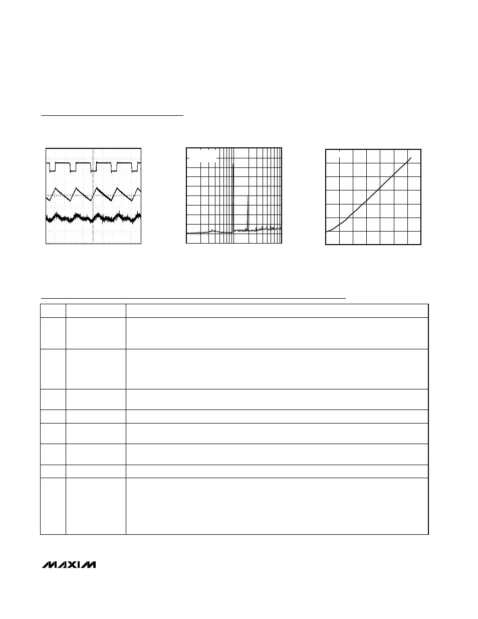
SWITCH CURRENT LIMIT vs. V
ISET
MAX1765 toc19
V
ISET
(V)
SWITCH CURRENT LIMIT (A)
V
OUT
= +3.3
Typical Operating Characteristics (continued)
(T
A
= +25°C, unless otherwise noted.)
LIGHT-LOAD SWITCHING WAVEFORMS
(V
IN
= +2.4V, V
OUT
= +3.3V, I
OUT
= 10mA)
MAX1765 toc17
A: LX NODE, 5V/div
B: INDUCTOR CURRENT, 200mA/div, AC-COUPLED
C: OUTPUT RIPPLE, 20mV/div, AC-COUPLED
A
B
C
500ns/div
450
0.1
1
10
LINEAR-REGULATOR OUTPUT NOISE
50
0
MAX1765 toc18
FREQUENCY (MHz)
NOISE (mV
RMS
)
150
250
350
I
LDO
= 200mA
V
LDO
= 2.85V