Max1765, Applications information – Rainbow Electronics MAX1765 User Manual
Page 16
MAX1765
used if ISET is employed to reduce the peak inductor
current (see Setting the Switch Current Limit and Soft-
Start). For high efficiency, choose an inductor with a
high-frequency core material to reduce core losses. To
minimize radiated noise, use a toroid or shielded induc-
tor. See Table 3 for suggested components and Table
4 for a list of component suppliers.
Output Diode
To assist startup with input voltages below 1.1V or
when V
OUT
is set for >4V, use a Schottky diode—such
as a 1N5817, MBR0520L or equivalent—between LX
and POUT (Figure 2). The Schottky diode carries cur-
rent after the synchronous rectifier turns off. Thus, its
current rating only needs to be 500mA. Connect the
diode as close to the IC as possible. Do not use ordi-
nary rectifier diodes; their slow switching speeds and
long reverse-recovery times render them unacceptable.
For input voltages over 1.8V, the Schottky diode may
improve light-load efficiency.
Input and Output Filter Capacitors
Choose input and output filter capacitors that will ser-
vice the input and output peak currents with accept-
able voltage ripple. Choose input capacitors with
working voltage ratings over the maximum input volt-
age and output capacitors with working voltage ratings
higher than the output. A 100µF, 100m
Ω, low equiva-
lent-series-resistance (ESR) tantalum output capacitor
is recommended for most applications. At the output of
the linear regulator (OUTL), use a 4.7µF ceramic
capacitor for stability at loads up to 500mA.
The input filter capacitor reduces peak currents drawn
from the input source and also reduces input switching
noise. The input voltage source impedance determines
the required size of the input capacitor. When operat-
ing directly from one or two NiMH cells placed close to
the MAX1765, use a single 33µF low-ESR input filter
capacitor.
The Sanyo POSCAP, Panasonic SP/CB, and Kemet
T510 are good low-ESR capacitors. Low-ESR tantalum
capacitors offer a good trade-off between price and
performance. Do not exceed the ripple current ratings
of tantalum capacitors. Avoid aluminum electrolytic
capacitors; their high ESR typically results in higher
output ripple voltage.
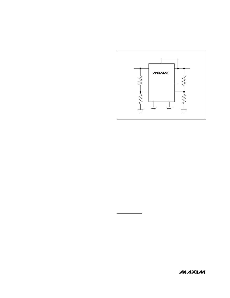
Bypass Capacitors
Bypass REF to GND with 0.22µF. Also, bypass OUT to
GND with a 0.68µF ceramic capacitor, and connect
OUT to POUT with a 4.7
Ω resistor. Each of these com-
ponents should be placed as close to its respective IC
pins as possible, within 0.2in (5mm).
Layout Considerations
High switching frequencies and large peak currents
make PC board layout a critical part of design. Poor
design will cause excessive EMI and ground bounce,
both of which can cause instability or regulation errors
by corrupting the voltage and current feedback signals.
Power components—such as the inductor, converter
IC, filter capacitors, and output diode—should be
placed as close together as possible, and their traces
should be kept short, direct, and wide. Connect the
inductor from the battery to the LX pins as close to the
IC as possible.
Keep the voltage feedback network very close to the
IC, within 0.2in (5mm) of the FB pins. Keep noisy
traces, such as those from the LX pin, away from the
voltage feedback networks and guarded from them
using grounded copper. Refer to the MAX1765 EV kit
for a full PC board example.
Applications Information
Use in a Typical Wireless
Phone Application
The MAX1765 is ideal for use in digital cordless and
PCS phones. The PA is connected directly to the step-
up converter output for maximum voltage swing and
power efficiency (Figure 10). The internal linear regula-
tor is used for postregulation to generate low-noise
power for DSP, control, and RF circuitry. The following
equations may be used to estimate the typical available
output current under conditions other than those listed
here:
800mA, Low-Noise, Step-Up DC-DC Converter
with 500mA Linear Regulator
16
______________________________________________________________________________________
Figure 7. Feedback Connections
MAX1765
INL
OUTL
POUT
OUT
FBL
FB
GND
PGND
R3
R4
R2
R1
STEP-UP
OUTPUT
LINEAR-
REGULATOR
OUTPUT