Rainbow Electronics MAX1765 User Manual
Page 13
tures a 250m
Ω, P-channel MOSFET pass transistor.
This provides several advantages, including longer bat-
tery life, over similar designs using a PNP pass transis-
tor. The P-channel MOSFET requires no base-drive
current. This reduces quiescent current considerably,
since PNP-based regulators tend to waste base-drive
current in dropout when the pass transistor saturates.
Connect the input of the linear regulator (INL) to POUT.
The linear regulator can be used to postfilter the switch-
ing regulator or regulate a separate supply voltage.
This regulated output is intended to power noise-sensi-
tive analog circuitry, such as low-noise amplifiers and
IF stages in cellular phones and other instruments, and
can deliver up to 500mA. Use a 4.7µF capacitor with
less than a 1
Ω equivalent series resistance (ESR) on
the output to provide stability. The linear regulator has
an internal 1.3A (max) current limit and thermal-over-
load protection circuitry to protect this output.
Configurations
There are several useful circuit configurations that can
be implemented with the MAX1765. The TRACK input
divides the circuit configurations into two types, one
where the DC-DC converter tracks to the LDO output,
and the other where the boost and the LDO regulate
independently.
Track Mode
Asserting the TRACK input places the MAX1765 into
track mode, where the DC-DC switching regulator’s
feedback pin (FB) is ignored, and the boost output
(POUT) “tracks” to 500mV above the linear regulator
output. The primary use of the MAX1765 in TRACK
mode is as a simple or very-low-noise step-up/down
power supply (see Figures 3 and 4; also see the
Maximum Output Current vs. Input Voltage plot in the
Typical Operating Characteristics.)
This circuit operates as a linear regulator when the
input supply (a battery) is greater than V
LDO.
When the
battery discharges below V
LDO,
the DC-DC converter
turns on, boosting POUT to a constant 500mV above
the linear regulator output. This configuration also
allows for true shutdown (see True Shutdown).
Dual-Supply Mode
When the TRACK input is low, the MAX1765 operates
two independent power supplies, a DC-DC converter,
and a linear regulator. One such application of this con-
figuration is shown in Figure 4. In this mode, the device
generates two boosted voltages from a single battery
supply. The DC-DC converter could be used to supply
the power amplifier (PA) of a cell phone, while the linear
regulator powers the baseband functions within the
phone. Asserting TRACK switches the device into track
mode when the high-voltage supply for the PA is no
longer needed, thus improving efficiency in standby-
receive mode. When the PA again needs 5V, deassert
the TRACK input.
Shutdown
The MAX1765 has a shutdown mode that reduces qui-
escent current to 1µA. During shutdown, the reference,
LDO, DC-DC converter, and all feedback and control
circuitry are off. Table 2 shows the MAX1765 shutdown
truth table. If ONA, ONB, and ONL are all deasserted,
the device is shut down.
True Shutdown
When a typical boost converter is placed into shut-
down, current can flow through the body diode of the
synchronous rectifier to the load. The MAX1765 can be
configured to allow true shutdown as shown in Figure 5.
The shutdown function is active low and is connected
to both ONA and ONL. When asserted, both the DC-DC
converter and the LDO are shut down simultaneously.
The LDO acts like a switch in this situation and discon-
nects the input from the load. Connect FBL to a resis-
tor-divider from V
REF
to GND (R3 and R4 in Figure 5) so
MAX1765
800mA, Low-Noise, Step-Up DC-DC Converter
with 500mA Linear Regulator
______________________________________________________________________________________
13
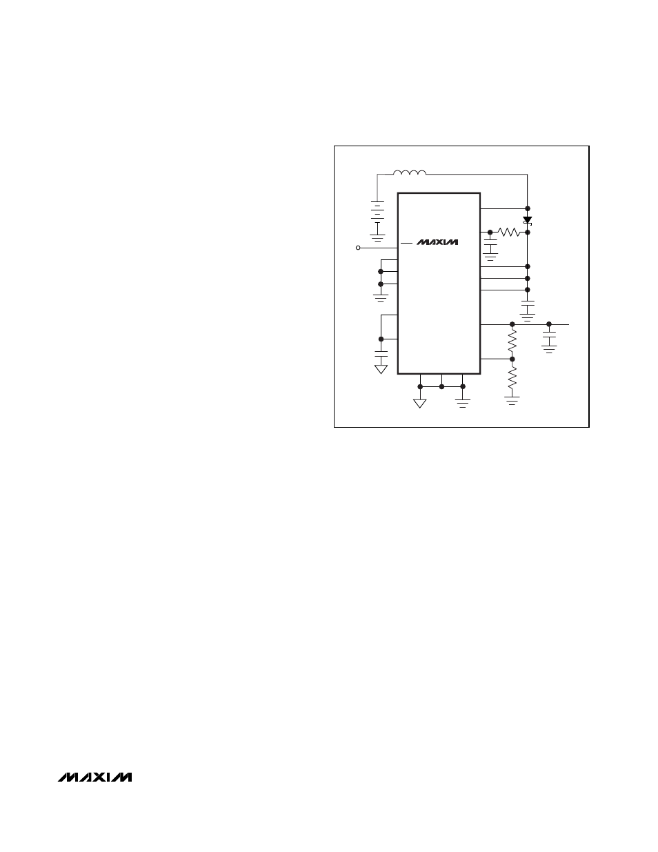
Figure 3. Simple Step-Up/Step-Down Converter
PGND
GND
MAX1765
FB
V
OUT
= 2.5V - 5.0V
AT 500mA
4.7
µF
33
µF
LX
OUT
POUT
TRACK
INL
OUTL
ILIM
REF
ONL
CLK/SEL
ONB
ONA
SHDN
INPUT
0.7V TO 5.5V
*
*
* OPTIONAL COMPONENTS
FBL
0.22
µF
*