Rainbow Electronics MAX2104 User Manual
Page 2
MAX2104
Direct-Conversion Tuner IC for
Digital DBS Applications
2
_______________________________________________________________________________________
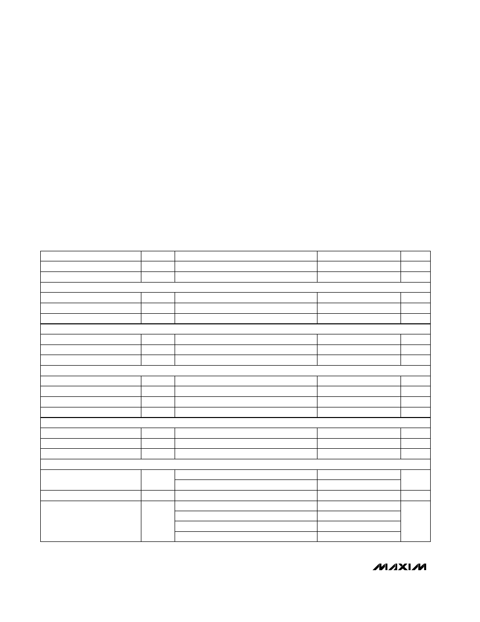
ABSOLUTE MAXIMUM RATINGS
DC ELECTRICAL CHARACTERISTICS
(V
CC
= 4.75V to 5.25V, V
FB
= 2.4V, C
IOUT_
= C
QOUT_
= 10pF, f
FLCLK
= 2MHz, RFIN_ = floating, R
IOUT_
= R
QOUT_
= 10k
Ω,
V
FDOUB
= V
INSEL
= V
CPG1
= V
CPG2
= 2.4V, V
PLLIN+
= V
MOD+
= 1.3V, V
PLLIN-
= V
MOD-
= 1.1V, T
A
= +25°C. Typical values are at
V
CC
= 5.0V and T
A
= +25°C, unless otherwise noted.)
Stresses beyond those listed under “Absolute Maximum Ratings” may cause permanent damage to the device. These are stress ratings only, and functional
operation of the device at these or any other conditions beyond those indicated in the operational sections of the specifications is not implied. Exposure to
absolute maximum rating conditions for extended periods may affect device reliability.
V
CC
to GND .............................................................-0.5V to +7V
All Other Pins to GND.................................-0.3V to (V
CC
+ 0.3V)
RF1+ to RF1-, RF2+ to RF2-, TANK+ to TANK-,
IDC+ to IDC-, QDC+ to QDC- ............................................±2V
IOUT_, QOUT_ to GND Short-Circuit Duration ......................10s
PSOUT+, PSOUT- to GND Short-Circuit Duration .................10s
Continuous Current (any pin)..............................................20mA
Continuous Power Dissipation (T
A
= +70°C)
(derate 27mW/°C above +70°C) .......................................1.5W
Operating Temperature Range...............................0°C to +85°C
Junction Temperature ......................................................+150°C
Storage Temperature Range ............................-65°C to +150°C
Lead Temperature (soldering, 10s) ................................+300°C
V
CPG1
= V
CPG2
= 0.5V
(V
MOD+
- V
MOD-
) = -200mV
(V
MOD+
- V
MOD-
) = 200mV
Referenced to V
CMO
Referenced to V
CMO
R
SOURCE
= 50k
Ω, V
FLCLK
= 1.65V
Referenced to V
CMI
Referenced to V
CMI
CONDITIONS
0.08
0.1
0.12
Charge-Pump Output High
Measured at FB
8
8
Reference Divider Ratio
33
33
Prescaler Ratio
32
32
mV
150
215
Output Voltage High (Note 3)
mV
-215
-150
Output Voltage Low (Note 3)
V
2.16
2.4
2.64
V
CMO
Common-Mode Output Voltage
µA
-5
5
Input Current (Note 1)
mV
100
Input Voltage High (Note 2)
mV
-100
Input Voltage Low (Note 2)
V
1.08
1.2
1.32
V
CMI
Common-Mode Input Voltage
V
4.75
5.25
V
CC
Operating Supply Voltage
µA
-1
+1
FLCLK Input Current (Note 1)
V
1.45
FLCLK Input Voltage Low
V
1.85
FLCLK Input Voltage High
V
2.4
V
IH
Digital Input Voltage High
V
0.5
V
IL
Digital Input Voltage Low
µA
-15
+10
I
IN
Digital Input Current
UNITS
MIN
TYP
MAX
SYMBOL
PARAMETER
mA
190
275
I
CC
Operating Supply Current
V
CPG1
= 0.5V, V
CPG2
= 2.4V
0.24
0.3
0.36
V
CPG1
= 2.4V, V
CPG2
= 0.5V
V
CPG1
= V
CPG2
= 2.4V
0.48
0.6
0.72
mA
1.44
1.8
2.16
STANDARD DIGITAL INPUTS (FDOUB, INSEL, CPG1, CPG2)
SLEW-RATE-LIMITED DIGITAL INPUTS
DIFFERENTIAL DIGITAL INPUTS (MOD+, MOD-, PLLIN+, PLLIN-)
DIFFERENTIAL DIGITAL OUTPUTS (PSOUT+, PSOUT-)
FREQUENCY SYNTHESIZER