Max781 pda/hand-held computer power controller – Rainbow Electronics MAX781 User Manual
Page 15
MAX781
PDA/Hand-Held Computer Power Controller
______________________________________________________________________________________
15
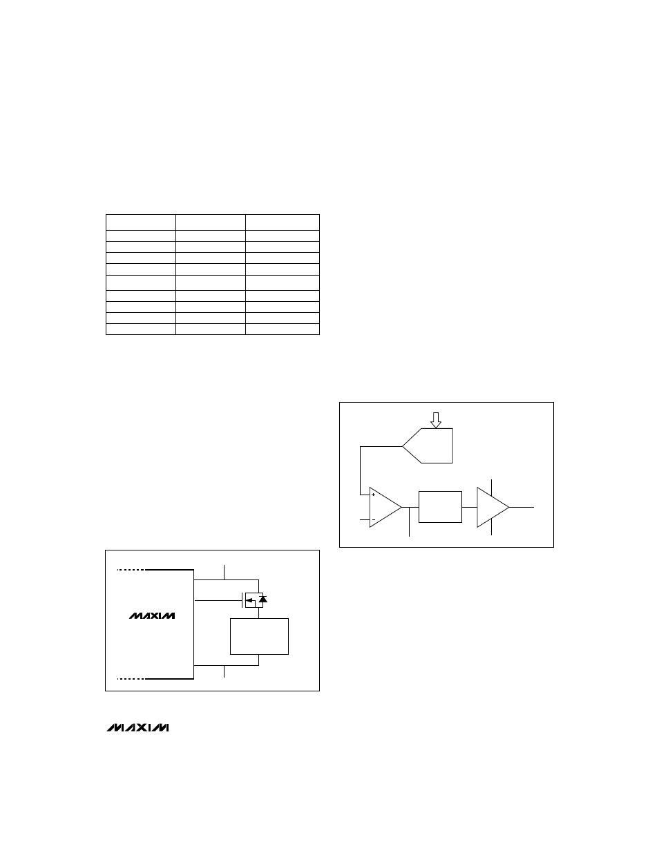
Gate Drivers
GD1 through GD5 are gate-driver outputs that high-
side drive external N-channel power MOSFETs. Loads
connected to 3OUT can be connected or disconnected
by using the circuitry shown in Figure 7. Clearing
GDSEL1 (GDSEL1 = 0) causes GD1 to sink up to
450µA to AGND. Setting GDSEL1 (GDSEL = 1) causes
GD1 to source up to 10µA from VHI. GD2–GD5 oper-
ate the same way. VHI is active (i.e., regulated to at
least 12.8V) only in operate mode, so the gate drivers
also only function in operate mode. GDSEL1 defaults
to a 1 on power-up. GDSEL2 through GDSEL5 default
to 0 on power-up.
FAST is a general-purpose output pin that sinks current
when FASTON = 1 and goes open drain when FASTON
= 0. FAST can be pulled up to any voltage up to 19V.
To use FAST as a general-purpose 3.3V logic output,
pull it up to 3OUT with a 100k
Ω
resistor. FAST may be
used to pull the gate of M3 down to connect the battery
to the input supply. The MAX781 does not limit the bat-
tery current when FAST is used in this way.
Battery Charger
The battery charger is a voltage-mode average current
regulator. Figure 8 shows a functional diagram of the
battery charger circuitry. The GMAMP is a transcon-
ductance amplifer with approximately 62dB of open-
loop DC gain. Set the GMAMP bandwidth with the
capacitor on COMP.
GMAMP bandwidth in hertz = gm / C
where gm = 0.0006 mho (mho = 1/
Ω
) and C = capaci-
tance on COMP in farads.
Average the current-sense signal by setting the
GMAMP bandwidth much lower than the battery-charg-
er switching frequency. The voltage output of the
GMAMP at COMP is converted to a duty cycle, which is
driven out of DCHG.
Serial-configuration bits CHG6–CHG0 set the average
current level. When CHG6–CHG0 are all set (1111111),
CSBAT is regulated to an average of 200mV. When
CHG6–CHG0 equals binary 0111111, CSBAT is regulat-
ed to an average of 100mV.
Analog Multiplexer
The MAX781’s built-in buffered analog multiplexer
selects one of eight different signal sources to be out-
put from the AOUT pin. Figure 9 shows the analog mul-
tiplexer circuitry. The AOUT buffer amplifier is disabled
in the shutdown and low-power modes, leaving the
89.7k
Ω
resistor to pull AOUT down to ground. Program
the MUX0, MUX1, MUX2 bits in the serial-configuration
data to select the analog multiplexer channel (Table 6).
Resistive dividers in the signal paths scale the chan-
nels to ensure that AOUT is scaled to REF. The AOUT
buffer amplifier can sink or source 1mA.
VPPA0
1
0
0
0
0
1
0
VPPA1
1
1
0
1
1
0
0
VPPB1
VPPB0
VPPA Voltage (V)
0
12
5
5
12
3.3
0
VPPB Voltage (V)
1
1
3.3
Table 5. VPPA and VPPB Control Bits
MAX781
3.3V LOAD THAT
NEEDS TO BE TURNED
ON/OFF
GD_
3OUT
N-CHANNEL
POWER MOSFET
...TO REST OF 3OUT CIRCUIT
...TO REST OF AGND CONNECTIONS
AGND
Figure 7. Using the Gate Drivers for High-Side Load Switching
GMAMP
DCHG
DCHG = 5OUT
EXTERNAL SWITCH OFF
DCHG = AGND
EXTERNAL SWITCH ON
5OUT
AT 0% DUTY CYCLE
,
DCHG = 5OUT
PGND
COMP
VOLTAGE TO
DUTY CYCLE
CONVERTER
7-BIT DAC
CHG6–CHG0
CSBAT
DACOUT
(0mV TO 200mV)
Figure 8. Battery-Charger Block Diagram