Max781 pda/hand-held computer power controller, Detailed description – Rainbow Electronics MAX781 User Manual
Page 10
MAX781
PDA/Hand-Held Computer Power Controller
10
______________________________________________________________________________________
_______________Detailed Description
Modes of Operation
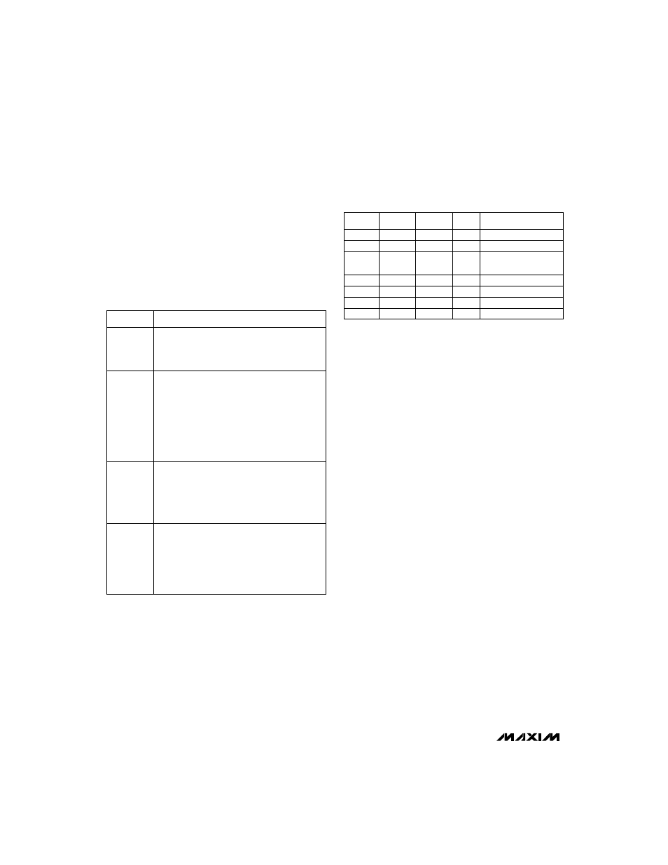
Table 1 describes the MAX781’s four modes of opera-
tion, and Table 2 shows how to select the desired
mode. MODE1 and MODE0 are the two bits, out of a
total of 32 bits of configuration data, which select the
operational mode. See Table 3 for a complete list of
the 32 bits of configuration data.
With
–
S
—
H
—
D
—
N
–
pulled up to the battery voltage, the
MAX781 powers on in low-power mode. After power-
up, pulling CE high temporaily places the MAX781 into
operate mode and allows data to be shifted into the
internal shift register. As soon as CE goes low, the
MAX781 enters the mode programmed by the MODE1
and MODE0 bits.
Serial Interface
The MAX781 is controlled by 32 bits of configuration
data. These 32 bits must be written, MSB first, into the
MAX781 using a synchronous serial interface. Table 3
describes the function of each bit of configuration data.
To turn the gate drivers on/off, select VPP voltages or
program the analog multiplexer. CE, SCLK, DIN, and
DOUT are the synchronous serial-interface pins. Figure
3 shows an example of the signal timing necessary to
send 32 bits of data to the MAX781. The first six bits
clocked out of DOUT are the status bits, and the
remaining 26 bits clocked out of DOUT should be
ignored. Figure 4 shows the detailed timing require-
ments of the synchronous serial interface.
To write the last eight bits of the configuration data
without affecting the rest of the configuration bits, clock
eight bits instead of 32 into DIN. This allows the
CHARGE, IDLE, MODE1, MODE0, and VPP control bits
to be updated in only eight serial clock cycles. As the
eight bits are clocked into DIN, the status bits are
clocked out of DOUT. Figure 5 shows an example of
such a quick access. If eight zeros are sent in a quick
access, no configuration data is updated. This allows
the status bits to be read quickly without affecting the
last byte of configuration data.
Status Bits
As the 32 bits of serial-configuration data are written
into the MAX781, 32 bits of data are read out of DOUT.
The first six bits contain status information, and the
remaining 26 bits should be ignored.
BATTINT and BATTSTAT (Table 3) indicate battery sta-
tus. It is assumed that the battery pack used with the
MAX781 has a thermistor attached to its negative termi-
MODE1
MODE0
0
x
x
1
1
1
–
S
—
H
—
D
—
N
–
1
0
1
1
1
0
1
0
0
1
0
1
CE
x
1
1
x
x
0
Resulting Mode
Shutdown
Operate
Standby
Operate
Standby
Low Power
1
1
1
0
Low Power (default
on power-up)
Table 1. MAX781 Modes of Operation
Table 2. Operating Modes
•
Buck switching regulator on
•
3OUT regulated to +3.3V
•
VPP outputs enabled
•
VHI regulated to +14V
•
Analog multiplexer enabled
•
High-side gate drivers enabled
•
Battery-charging current source enabled
Operate
•
Default on power-up
•
3OUT supplies 10mA at +3.3V linear
regulated from BATT
•
VPP outputs off (VPPA = VPPB = High-Z)
•
Analog multiplexer off (AOUT = High-Z)
•
High-side gate drivers off
(GD1 = GD2 = GD3 = GD4 = GD5 = 0V)
•
Battery-charging current source off
(DCHG = 5OUT)
Standby
•
3OUT supplies 10mA at +3.3V linear
regulated from BATT
•
VPP outputs off (VPPA = VPPB = High-Z)
•
Analog multiplexer enabled
•
High-side gate drivers off
•
Battery-charging current source enabled
Low
Power
•
Entire chip shut down
•
All blocks turned off
•
I
Q
< 10µA
•
3OUT, 5OUT, REF off
Shutdown
MODE
DESCRIPTION